Topological insulators are a special class of materials that do not conduct electricity but allow it to flow along their surface. Their key feature is topological protection: even in the presence of defects, irregularities, or sharp bends in the material, electrons continue to move without scattering or losses. This fundamental property is used to create robust electronic devices, such as sensors, memory devices, and quantum computers.
In their work, the researchers used the principle of topological protection in photonics – the field where data is transmitted using photons rather than electrons. Unlike electronic circuits, photonic systems do not heat up; they operate at higher frequencies and can significantly improve the energy efficiency and carrying capacity of computing devices. These advantages make photonic technologies especially popular amid the constantly growing computational loads and energy consumption in modern data centers, driven by the rapid development of AI. However, to create new photonic computing architectures, we need to learn how to effectively control light on scales smaller than the wavelength in all directions.
Back in 2017, ITMO scientists as part of an international team predicted the existence of a 3D photonic topological insulator and described its physics. After that, the key task was to create a 3D structure because it provides a greater freedom for the trajectories of electromagnetic wave propagation compared to one-dimensional and two-dimensional systems – and thus more flexible control of light on a chip. However, for a long time, it was believed that creating such an insulator was practically impossible. It was believed that surface photonic states at the boundary with air would lead to energy leaks and destruction of topological stability, ultimately preventing the insulator from functioning properly.
Thus, ITMO researchers became the first to come up with a fully dielectric (not conducting electricity) 3D photonic topological insulator. Unlike metal photonic structures that heat up and are hard to scale, the dielectric insulator doesn’t have these limitations.
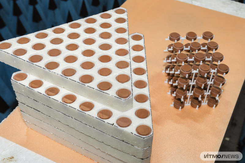
All-dielectric photonic topological insulators. Photo by Dmitry Grigoryev / ITMO NEWS
The experimental structure is a multilayer dielectric system that resembles a layer cake. Each “layer” contains a dozen ceramic dielectric components. Thanks to their unique geometry, photons on the insulator’s surface acquire pseudospin – an analog of electron spin in topological insulators. Pseudospin is connected to polarization and determines the direction of light propagation in the topological structure: light with right circular polarization will travel along all layers of the insulator's right side edge, while light with left circular polarization will go along the layers of the left side edge. Thanks to this property, it is possible to direct electromagnetic waves by simply switching the source’s state. Upon reaching the insulator’s corners, the light is collected at the edge and emitted into free space.
Another unique property of an all-dielectric 3D photonic topological insulator is the topological robustness of surface photonic states. Even when some structural elements are removed or the structure is damaged, surface waves continue to propagate without losses, passing around the defects. This makes it possible to form arbitrary light propagation trajectories and control the direction of radiation without the need to perform a complex reconfiguration of the entire system.
“We demonstrated that what was formerly considered a loss can actually become a functional advantage. By using the open surfaces of the 3D topological insulator, we learned to control the radiation direction and wave routing by manipulating pseudospins. This is a brand-new tool for creation of new photonic devices and optical chips,” shares Dmitry Zhirikhin, the paper’s first author and a senior researcher at ITMO’s Faculty of Physics.

Dmitry Zhirikhin. Photo by Dmitry Grigoryev / ITMO NEWS
The new insulator can be used to develop compact, high-capacity, energy-efficient, and robust photonic integrated circuits and optical chips. It’s a promising alternative to conventional electronic devices that may serve as a hardware foundation for faster AI architectures.
Importantly, the new device is scalable and can be adapted to a wide range of wavelengths, which makes it a versatile platform for photonic integration. In the future, the team is planning to create smaller versions of the insulator, compatible with photonic integrated circuits and optical chips, as well as study new geometries that can control light with even more flexibility in 3D computational architectures.
This study was supported by the national program Priority 2030 and Russian Science Foundation (grant No. 24-72-10069).