Vladimir Dubrovskii, head of Laboratory of Physics of Epitaxial Nanostructures at ITMO University and head of a research project at European XFEL
What were the main topics of discussion at this conference?
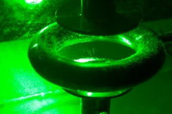
One topic was research on filamentary nanocrystals (nanowhiskers) and nanowhisker-based heterostructures grown on silicon wafers. Another one, and that is a very trendy topic right now, is the project NanoMAX, which is currently carried out at the University of Paris-Saclay, and in which ITMO University also participates. The project revolves around using a transmission electron microscope to grow nanowhiskers and film the process at atomic scale. We can actually see how the crystal lattice is formed, how its parameters, chemical make-up and other parameters change. It’s absolutely unique; I’ve been working in this field all my life and if someone were to tell me about this 10 years ago, I wouldn’t believe them. The third main topic concerned the use of XFEL in studying semiconductor nanostructures for use in photonics.
Can you tell us about your project at XFEL?

We begin work on our project at XFEL in October. We’ve been provided a period of time in which we can use the laser to study nanowhiskers, and, to be precise, high-speed processes in their crystal lattice under the impact of ultra-short, high-energy pulses of coherent laser light. Right now we’re preparing samples, i.e. growing nanocrystals using molecular-beam epitaxy, which we do together with our colleagues from Spain and France. XFEL will be beneficial to the optimization of nanostructures which will serve as a basis for more efficient devices that will be part of the so-called “green photonics”.
And this can only be done with XFEL?
Yes, that is the only place where we can produce the necessary physical conditions. XFEL is not just a tool for semiconductor research. The system produces radiation fields so powerful that they can be used to create materials of extreme density, the kind that doesn’t occur on the surface of Earth and is only present in its core. This means we can study the physics and chemistry of previously unavailable states of matter. It’s the same with high-speed processes because the growth dynamic of a crystal lattice is incredibly fast.
Robert Feidenhans'l, managing director of XFEL (Germany)

What are your reasons for participating in this conference?
I have a personal interest in nanowhiskers; I’ve worked in that field for 10 years, and this conference is a great chance to learn all about what is currently popular in this area and what progress has been made over the recent years. I’m interested in what has to do with the methods of manipulating and growing nanowhiskers. It’s astounding what a massive leap has been made in the past 10 years of research. We’re already talking about numerous potential applications of this technology, and that is very promising.
What do you think made this leap possible?
There are four factors. The first is the development of new equipment. The second is the advances made in process modeling, because you need to know how nanocrystals grow. The third is the development of resources used to characterize the processes and materials, i.e. the active use of electron microscopy, X-ray technology, and other tools. Finally, the fourth factor is the awareness of all the potential applications for projects in this field, which further stimulates new research.

XFEL has now been operating for more than six months. What results are there so far?
The first experiments began in September, and I’ve just received the first results, which will soon be published. Right now we’re focused on two of the laser’s instruments, which are used for structural biology and femtosecond chemistry research; you could say that these are the top-priority areas of research for us. We’ve already got some very good results in this area. One of the major goals is to understand the specifics of molecular movement in various reactions, and the first steps have already been made. We’ve also just finished the second competition that will determine how much time with the laser will be allotted to each scientific team, among which are, too, several nanowhisker research projects. Teams that participated in this selection will start their work in October, and the third competition will start in mid-May and last through June.
XFEL has recently held its first Open Day. How did that go?
It was highly successful. We were careful about the announcement as we were afraid that there would be too many guests. A total of 2,500 people came to our facility. We showed them around the labs, the engineering tunnels, and conducted an experiment during which they could see how lasers work and witness different magnetic phenomena. We also had some special events for kids. It’s really important to show people just what we do at XFEL and to popularize science in general.
Ray LaPierre, chair of the Department of Engineering Physics at McMaster University (Canada)

What made you come to Nanostructure for Photonics?
There are a lot of researchers here who work in fields related to my own. I collaborate with many of those present here, including Vladimir Dubrovskii, with whom we plan to work on a student exchange program. I’ve also brought my PhD students here. And, of course, getting to see St. Petersburg is already enough of a reason to come here.
You were one of the event’s speakers. What was your report about?
I’m working on devices that will see active use in a decade or so. Those are new photodetectors, cheaper and with better sensitivity, materials for infrared cameras that can be used to detect heat sources just by putting on a pair of glasses, and nuclear batteries that can work on a single charge for 100 years. There is a radioactive source inside them that creates a stream of electrons that loop back on themselves with the help of nanowhiskers. We’re also working on solar power elements. All these devices are based on nanowhiskers, i.e. filamentary nanocrystals. When photons penetrate such a structure, they become “trapped”. That’s why these materials seem very black in color, because they reflect very little light. This quality helps us make highly sensitive light sensors and other practical devices.
Which of these projects do you find the most inspiring?
In the past two years, we’ve been very excited about our work on nuclear batteries. There are some models out there on the market, but they aren’t very efficient. These batteries have a lot of applications in areas where regular energy sources aren’t enough. For example, airplane “black boxes” can only last 30 days with modern energy sources. A nuclear energy source would last much longer.
Frank Glas, Centre for Nanoscience and Nanotechnology at University of Paris-Saclay (France)

What makes Nanostructure for Photonics special is that it is education-oriented: students take an active part in the event and there are workshops here. Even though there are only 60 participants and only half of them present reports, you have students from many different fields here. This presents opportunities for interdisciplinary research, although many of them are already working together. I think the guests were very impressed with the results of the NanoMAX project that were presented here. Theoretical scientists have long dreamed about this, and it’s a very beautiful thing.


