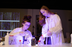
The world is full of magic for those who don’t know physics. And we know that physical laboratories can be more charming than sorcery. Just look at how Semyon Bachinin, a junior researcher at the Faculty of Physics, conducts an experiment involving the optoelectronic response of a copper oxide crystal. The results of his work are similarly impressive!
Copper oxide, also known as tenorite, is a widespread natural semiconductor. Researchers at ITMO were able to use it to create an artificial optical synapse. It turns out that when subjected to laser radiation, tenorite crystals demonstrate a behavior similar to that of the neurons in our brain: their reaction to radiation depends on the frequency of laser pulses, just like synapses react to neuromediators. This technology can lay the foundation for a new type of processes that imitate biological neural networks. In the future, this method could be used to accelerate computations and train AI algorithms, while also reducing their energy use. The results of the study were published in ACS Applied Materials & Interfaces.

Photo by ITMO’s Faculty of Physics
Meanwhile, this mesmerizing glowing blue-green globe is a vial containing the products of perovskite inorganic quantum dot synthesis. These are nanocrystals measuring 5-10 nanometers in size with record-high quantum efficiency (up to 95-98%). In simpler terms, this means that up to 95% of the energy incident on the quantum dots in the UV range is re-emitted in the visible range with minimal losses. Such quantum dots are not just beautiful: by synthesizing new perovskite nanomaterials with a specific composition and shape, scientists should be able to create miniature laser light sources. In turn, this opens up tremendous opportunities for quantum technologies, the development and implementation of advanced biosensors and next-generation sensors, flexible electronics, and much more.
Studies of this kind are conducted at ITMO’s Laboratory of Hybrid Nanophotonics and Optoelectronics (PeroLab). For instance, recently, the lab’s team partnered with scientists from Moscow Institute of Physics and Technology to create the world’s smallest blue laser. With a volume 13 times smaller than the wavelength of the produced light, it paves the way for the creation of a new generation of ultra-high-resolution displays and compact biomedical devices.

Photo by Dmitry Sbytov, Artemy Averiyanov, and Kirill Borozdin / Infochemistry Scientific Center

Photo by Dmitry Sbytov, Artemy Averiyanov, and Kirill Borozdin / Infochemistry Scientific Center
An equally bright (pun intended!) future is predicted for crystals of organic fluorophores (substances that absorb and emit light) – you can see them in the picture above. These crystals were synthesized by researchers at ITMO’s Infochemistry Scientific Center for use in spectral research and the creation of new materials. Curiously, these images were made with the tools at hand: a smartphone under UV light (with a wavelength of 365 nanometers).
Organic fluorophores are the object of experiments conducted by the team Chemistry of Organic Molebytes, which includes PhD student Dmitry Sbytov and two second-year Bachelor’s students, Artemy Averiyanov and Kirill Borozdin. Kirill and Artemy came to the lab for an internship and have already joined its ongoing projects. The group is headed by Anton Muravev, an associate professor at the Infochemistry Scientific Center. Together, they are developing a new type of chemical sensors – organic compound-based fluorescent detectors that can quickly and accurately assess the presence of toxic metals (such as lead, cadmium, or mercury) in water or soil. Heavy metals enter the environment from various sources: industrial emissions, agricultural runoff, and household waste. Once in water or soil, they accumulate and cause severe, often irreversible, consequences for ecosystems and the health of humans and animals – including damage to vital organs and serious diseases.
The new sensors developed by the team will act like “chemical lightbulbs,” coming alight to warn users of the presence of dangerous substances. At the same time, unlike existing detection methods, they will make it possible to conduct an express analysis on site, without complex equipment.

Photo by Pavel Alexeevsky, Alyona Kulakova / ITMO’s Faculty of Physics
And these are different crystals – those of a metal-organic framework with a complex formula: [Cd₂(TCPB)(azopy)₀.₅(DMF)]. It is made up of cadmium (Cd) atom nodes connected by organic molecules TCPB and azopy, the “building blocks” of the crystal structure. The solvent (DMF) fills the pores when the material is synthesized.
Metal-organic frameworks (MOFs) are a special type of hybrid materials. Their lattices are made from metal ions that are connected by organic ligands (specific atoms, ions, or molecules) – hence their compound name. For scientists, MOFs are a platform for designing materials from scratch. Like architects, specialists in this field can pick a metal, design an organic connection of the needed length and functionality, and get a material with strictly specified properties for a particular task. At the same time, there are many tasks that can be potentially solved with MOFs. For example, these materials can be used to create highly precise gas analyzers to detect leaks of hazardous gases in laboratories or production facilities in a timely manner. Additionally, significant prospects are associated with their use in optical components of laser systems.
Scientists at ITMO’s Faculty of Physics work with MOFs; they took this picture at a lab during their study of optical birefringence in such materials (this is an optical effect in which light, passing through a transparent anisotropic crystal, splits into two beams with different polarizations and propagation speeds). This image was acquired with a ZEISS optical microscope with 25x magnification, which allows us to see the form and “purity” of crystals in the visible range.
Materials with pronounced birefringence are essential for creating key elements of laser and photonic systems: polarizers, modulators, and optical filters. However, traditional crystals have several limitations, including narrow spectral range, relatively weak birefringence, and internal defects. In their work, researchers from ITMO have suggested a new approach to creating optically anisotropic materials (those whose properties depend on the direction of influence) by targeted changes of MOF composition and structure. Thanks to this approach, optical properties of crystals can be precisely adjusted, thus expanding their applications in photonics and laser technologies.
This study was conducted at the Faculty of Physics by the team of Valentin Milichko and authored by Svyatoslav Pivovarov and Alyona Kulakova, researchers at the faculty. Their work was supported by the Russian Science Foundation grant No. 23-73-01235 and the Priority 2030 program.

Photo by Dmitry Grigoryev / ITMO NEWS
Both physicists and chemists work on methods that would allow us to create materials with specific properties. Scientists at ITMO’s Infochemistry Scientific Center have developed another approach to the task. They have figured out how gradient structures of cobalt compounds form when Liesegang rings emerge in agar gel – you can see the result of this experiment in the photo. In the future, this approach will make it possible to rapidly and affordably produce new materials with tailored properties. These can be used as substrates for cells in electrochemical devices, thermal sensors, and antimicrobial coatings. Find more details about the study in this article.

Photo by Dmitry Grigoryev / ITMO NEWS
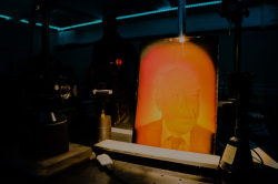
Working with glass also has its challenges. It’s quite a fragile material that is sensitive to temperature changes. The functionality of regular glass can be improved with an additional metal layer; this makes it possible to create electronic elements, as well as mark or decorate glass.
However, it’s not that easy to give glass such an “upgrade.” At ITMO, this problem has been solved with a physical and mathematical model for predicting the parameters of laser metal transfer on a glass substrate. Apart from providing a detailed model of the physical process, the new tool can predict its key parameters with a 90% accuracy. This opens up possibilities for the controlled creation of metallic coatings with micron-level resolution on glass, such as indelible protective marks and decorative elements. The photo above demonstrates the results of this study. You can read more about it in one of our previous articles.

Photo by Olga Kushchenko / Faculty of Physics
At a lab, you can even see something that’s typically invisible. Here’s one striking example: a white laser’s diffraction in a quasicrystal. The quasicrystal is just 120 micrometers in size (the width of a human hair!). The white laser beam (supercontinuum) passes through this structure, then diffracts, and as a result we can see the image captured by Olga Kushcheko, an engineer at ITMO’s Faculty of Physics.
Quasicrystals are remarkable materials that once shattered all the classical rules of crystallography. It was previously believed that only periodic order was possible in solids. But scientist Dan Shechtman discovered a structure with the symmetry forbidden for crystals (a fifth-order axis, like that of a pentagon) in an aluminum-manganese alloy. For this discovery, he received the Nobel Prize in 2011. In the future, the use of quasicrystals could unlock new possibilities in creating lasers and sensors.
This topic is actively explored at the Faculty of Physics. For instance, researchers there have already managed to “capture” light in a polymer quasicrystal.