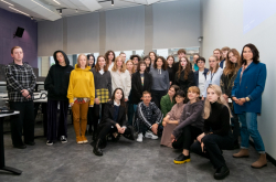
Specialists in laser technologies are in demand in various industries. This field includes many specializations and at ITMO University, the Master’s program in laser technologies is subdivided into several tracks that students get to choose from in their second year of studies:
-
Specialization Laser Micro- and Nanotechnologies focuses on physical and technological foundations behind laser technologies and their applications in scientific research.
-
Students in the Laser Biomedical Technologies specialization get to learn how to apply laser technologies in biomedicine, e.g., laser surgery, cosmetology, and dentistry.
Last year, the third track, Industrial Laser Technologies, was launched. Master’s students in their second year of studies who chose this specialization will learn how to do laser cutting, welding, and fusing, as well as create various laser sensors and other devices for industrial purposes.
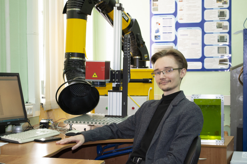
“Graduates of the first two specializations will be able to develop projects at Technology Readiness Levels (TRL) two and four. As for the third specialization – we’ll train professionals who’ll be able to improve a laser device from TRL three to TRL six. This means that they’ll be able to not only come up with a physical and technological concept and design a prototype, but also demonstrate it’s viability in real-life conditions and prepare it for implementation at a facility,” says Dmitry Sinev, a lecturer at the Laser Technologies Master’s program.
Dmitry Sinev. Credit: Dmitry Grigoryev, ITMO.NEWS.
Study plans
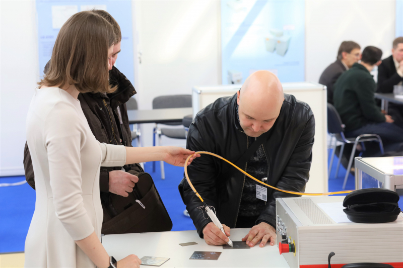
Students who choose the industrial specialization will learn about laser-induced thermal processes in condensed media, optical and technical systems of technological lasers, and modern industrial laser technologies. Lecturers from the Faculty of Nanoelectronics will give classes and invited speakers from the Laser Center and NPP Signal companies will share their experience of design and engineering in laser technologies and modern scientific and technical challenges of this industry.
“During their studies, our students will work on applied research topics, such as the creation of electronic elements using the laser-induced copper deposition method from deep eutectic solvents or the study of polymer markup under ultraviolet laser radiation. In other words, it’s either about working on the implementation of already researched technologies in the industry, or solving technological tasks of a partner company,” says Dmitry Sinev.
After graduation
Graduates of the industrial specialization will be able to land jobs in various fields – for example, they will be able to become design engineers and researchers in R&D departments of high-tech companies, technologists for laser materials processing, service engineers, laser equipment operators, or analysts. Internships and permanent positions in this field are offered by Russian and international partner companies of the Master’s program, including Laser Center, NPP Signal, Leningrad Laser Systems, and IPG Photonics, as well as manufacturers and suppliers of photonics elements, such as Azimut Photonics, Avesta Project, Inscience, and many others. Moreover, students and graduates can launch their own startups with the support of the Laboratory of Micro- and Nanotechnology Lasers.
Projects by Master’s students
First-year Master’s students who have chosen the industrial track will attend a series of lectures on the topic of laser technologies in the industry during the upcoming academic year. In addition, they chose specific applied tasks together with representatives of companies: some of them were proposed by the partners and others by research advisors. During their second year of studies, the students will have to propose ways to solve the given problems and defend their solutions as theses. They shared their projects and future plans with ITMO.NEWS.
Alexey Chebotarev

Alexey Chebotarev. Photo courtesy of the subject.
I feel like Industrial Laser Technologies is a more practice-oriented specialization, as part of which I’ll get to work with different companies. Another advantage of the industrial track is the opportunity to write my thesis about the device I’m working on at my workplace, NPP Signal.
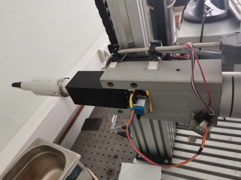
I’m developing a laser sensor for the detection of small metallic objects the size of 200 microns (0.2 millimeters). The thing is, nowadays the devices are getting smaller, and correspondingly, so do their parts. Because of their size, it’s easier to overlook a part while assembling a device, which will result in defects.
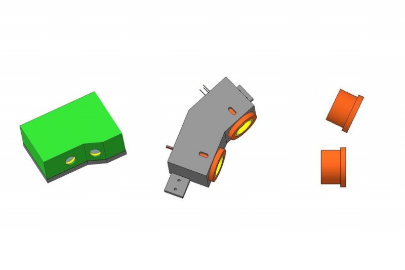
3D model of the laser sensor prototype. External part on Pic.1 and internal parts on Pic.2 and 3. Laser raditation gets focused using a lense (the lower orange cylinder) in the studied area. If there's an object there, the radiation reflects from it and gets captured by the second lense (the orange cylinder above), which focuses it on the photoreceiver. Image courtesy of the project's author.
There are many different ways to check if devices are assembled correctly. One of them is machine vision, but equipment required for that is extremely expensive. We want to create a more cost-effective solution that doesn’t require complex additional software. Our laser sensor can be put on the assembly line and it will analyze whether all the parts in the mechanism are in place. If something is missing, it will produce a signal. This will help better control the quality of devices, for instance, protect them from arcing, control the development of reed switches, or the degree of wear of the tip that makes holes in ceramic microcircuits.
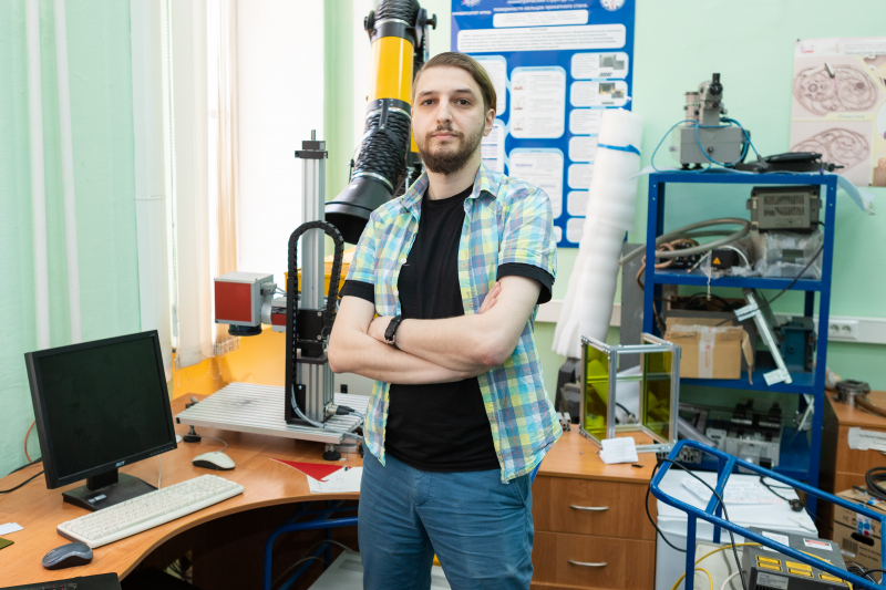
Evgeny Prokofiev
Evgeny Prokofiev. Photo courtesy of the subject.
After an internship at Laser Center, I became interested in industrial projects and decided to work in this field – that’s why I chose the new specialization. My research advisor Galina Odintsova suggested I study laser-induced periodic surface structures (LIPSS) in materials, which isn’t an easy task.
Prototype for the control polarization module. Photo courtesy of Evgeny Prokofiev.
To create such surfaces with a laser beam, you need to change its parameters. It’s impossible to do this only with the help of the MiniMarker 2 laser installation, since it doesn’t have the required optical elements. Therefore, it’s necessary to use additional equipment that we’ve developed – a module with prisms, lenses, and other optical elements. It works as follows: the laser beam enters the module from the collimator where it changes its parameters. After this, we can program the image we need and the modified beam will etch a holographic image that looks like an iridescent sticker on the sample.
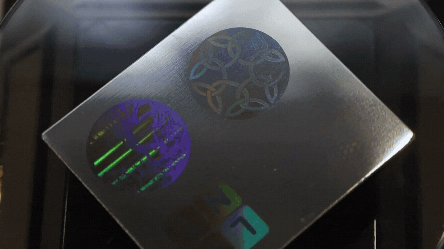
Demonstration of irridicent microstructures that can be achieved using the proposed module via the laser installation MiniMarker 2. Video courtesy of Evgeny Prokofiev, the author of the project.
LIPSS have been researched by scientists for over ten years, but not in the industry. Representatives of the Laser Center are interested in our project and plan to use the achieved results, for instance, to fight forgery. Household appliances are usually marked with stickers representing their manufacturers but they aren’t durable, while laser etching won’t go anywhere.
Stepan Pukalov
Stepan Pukalov. Photo courtesy of the subject.
As a Bachelor’s student, I did an internship at the Leningrad Laser Systems company. I liked it so much that I wanted to stay there. As a result, it so happened that now in the Master's program I’m engaged in industrial lasers, while at the workplace my activities are related to highly-powerful lasers and materials processing – welding, cutting, marking, and surfacing of metals and non-metals. I’m sure that industrial laser technologies is a very promising field, especially in the current situation, when it’s possible to develop the Russian laser industry.
In my Master’s program, I’m studying laser heat strengthening of titanium using graphite powder. The thing is, in the laboratory we can increase the microhardness of small areas of the material but how can we densify larger, irregularly shaped industrial objects? In addition, the solution must be economically justified, because it’s quite expensive to use industrial installations and graphite powder.
We suggest using robotized installations by Leningrad Laser Systems. We can cover the titanium plate with graphite powder and then melt it with a high-power laser. Titanium and carbon will mix resulting in solid titanium carbide. We are still to come up with a way to radiate the graphite-covered titanium with lasers from all sides. The technology will be suitable for application in various fields to create resistant materials, for instance, in military industry, construction, transportation, or medical equipment, such as tools and prostheses. Moreover, titanium is sensitive to friction, while titanium carbide isn’t. This property can be used in various mechanical systems that deal with lots of friction, such as engines, to increase their longevity.
You can learn more about the Laser Technologies program and entrance exams here.