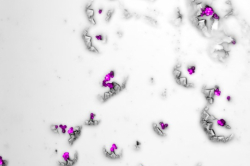
The photo was taken with a Tescan scanning electron microscope. You can spot the growth of the surface charge changing when the crystal’s surface is irradiated with an electron beam.
In the course of the irradiation, an excess charge is accumulated on the surface of lithium niobate, which leads to the emergence of a strong electric field and the subsequent movement of the domain wall. A domain wall is an area with an interruption of the order of the crystalline lattice along which the contact of two differently directed domains takes place. Such areas can hold mobile charges. In the image, the bright “arrows” characterise areas with strong charges that accumulate on the edges of domain walls.
The research on the structural properties of lithium niobate and lithium niobate-based optical waveguides is being conducted by the Laboratory of Assembly and Alignment of Light-Guided Photonics Devices as part of the fundamental research project “The study of the physical mechanisms and the nature of noise in integral optical circuits and their effect on precision optical measurements”. The research focuses on a deeper analysis of lithium niobate-based integrated optical modulators, and is aimed at stabilizing properties of modulators.
According to the scientists, the results of this research can be promising in regard to the use of lithium niobate crystals for signal processing in high-precision sensors.