Each material has a different nanorelief (irregularities, protrusions, or cavities on the surface) that affects its optical properties. For instance, one surface is better at harvesting and reflecting light, while another will have a limited emissivity. Each property has its own applications: materials with a light-harvesting nanorelief are used in solar cells, while reflective surfaces are used to create iridescent patterns that protect products from counterfeiting.
Typically, photolithography is used to create ordered nanoreliefs. This method is reminiscent of using spray paint with a stencil: first, a template is made for the target image; then, it is recreated on a material by shining a laser through the template. However, photolithographs are expensive and require a lot of expendable materials, such as templates and photoresists (materials that react with laser radiation to register an image). Moreover, with this technique, it is impossible to change the image when writing is in progress – instead, that would require an all-new template.
An alternative technique is direct writing with scanning laser beams. It doesn’t require expensive equipment or expendable materials, while also being capable of creating smaller structures, as if drawn by a thin brush. Researchers from ITMO’s Institute of Laser Technologies have further improved this approach by introducing a method for generating laser-induced periodic surface structures (LIPSSs). The method can be used to distinguish, print, and combine even smaller nanostructures within the scanning area.
“As the material has a rough surface, the laser radiation that reaches it diffracts and turns into an electromagnetic wave that spreads along the surface and interacts with incoming laser radiation. As a result, we get a nanorelief in the shape of a protective pattern. Imagine that laser radiation is a wide brush around 55-70 microns in size. And in this brush, different lines are created by filament, each just 0.7 micrometers in size – that’s 100 times thinner than a human hair. These filaments create tiny nanostructures inside the big structure,” explains Dmitry Sinev, an associate professor at the Institute of Laser Technologies.
Protective trademarks formed via direct writing of laser-induced periodic surface structures. Video courtesy of Dmitry Sinev
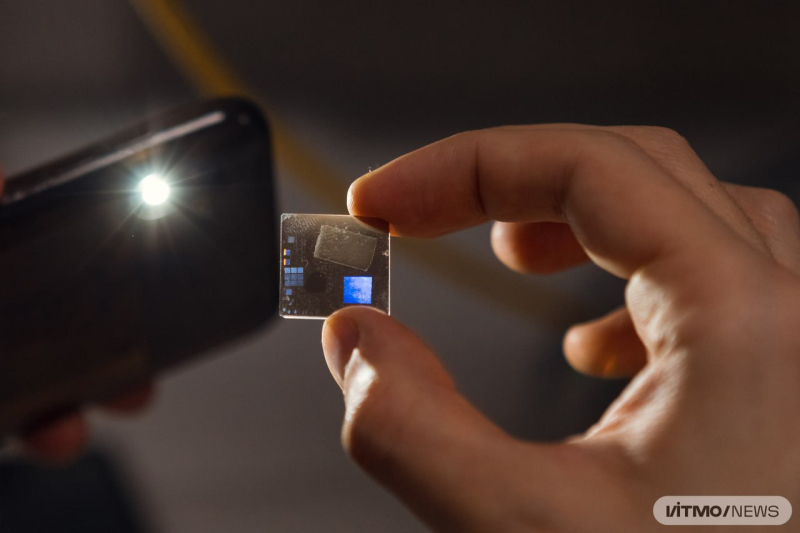
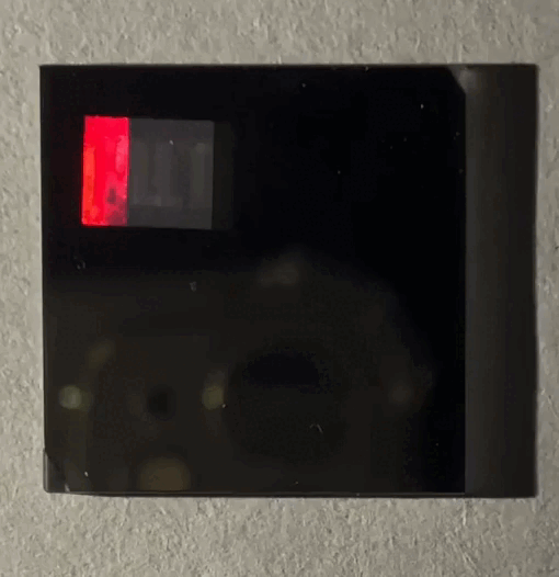
The new method works as follows: a titanium film is placed upon a glass substrate; then, the film is treated with a laser beam that creates a one-dimensional nanorelief in the shape of several lines. In order to make the geometry more complex and turn the image into a 2D one, the process of forming lines is repeated, with a new set of lines drawn across the first one. The final nanorelief is reminiscent of honeycombs and squares and can be seen in white light, like that from a flashlight.
“Through repeated processing, the nanoreliefs took the thermophysical and mechanical properties of the substrate, as well as the optical properties of the film – this changed their interaction with polarized light, as well as refraction and light transmission spectra. Each nanostructure in a pattern shone with different colors of varying intensity based on the angle it was viewed from. Upon request from a customer, we can write any image with additional customization. For instance, we can create a nanostructure that will be brighter at a specific angle, and inform the customer about the configuration parameters. This way, only the customer will know the location of each element and thus will be able to identify the pattern,” adds Alexander Suvorov, a second-year Master’s student at the Institute of Laser Technologies.
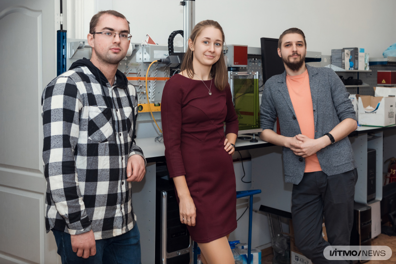
The paper’s authors (left to right): Alexander Suvorov, Yaroslava Andreeva, and Dmitry Sinev. Photo by Dmitry Grigoryev / ITMO.NEWS
According to the paper’s authors, the pattern can be made even more unique if several protective layers are combined in its production: for instance, the image can be writtenin 2D and in 1D.
Next, the researchers are planning to use their method to make colorful trademarks that will prevent counterfeiting of medical vials, test tubes, and other products made from transparent materials. Currently, the novel method is capable of printing protective patterns with the resolution of 0.7 microns and the area of 1x1 millimeters in just 18 seconds. In the future, the researchers are planning to increase the writing speed and make the nanostructures smaller, in order to include more elements and make the image even harder to copy.
This research project is supported by the Russian Science Foundation.