Two-dimensional materials in photonics
The creation of efficient light control systems is one of the major challenges for photonics today. Nothing in the universe is faster than light. That is why researchers have long cherished the idea of using photons to transmit data and create computing devices that would outperform the existing ones by tens or even hundreds of times.
However, prior to that, they need to overcome several obstacles. To begin with, light is difficult to control. Photons tend to scatter into the environment and what is more – they cannot interact with one another.
As it turned out, the solution can be found in the new 2D materials. The first article about graphene saw the light of day back in 2004. As of now, researchers have already discovered a hundred more similar mediums. Among them are materials acting as electronic topological insulators, superconducting materials, and semiconductors that may offer alternatives to classical semiconductors like silicon, which is commonly used in electronics.
The key advantage of a large class of 2D materials lies in excitons. These are special quasiparticles that consist of a negatively charged electron and a positively charged electron hole. They are controllable, can be easily excited by light, and have a strong optical response.
Both light and matter
With further research, scientists figured out how to produce a different type of quasiparticle. Polaritons are hybrid particles made up of excitons and photons, which means that they demonstrate properties of both. The quasiparticles appear as a result of the multiple regenerations of photons into excitons and back again triggered when a 2D semiconductor is placed in an optical resonator calibrated to the frequency of an exciton. During the experiments, the authors of the paper proved once again that nanostructured metasurfaces can be used instead of a resonator, too.
“The thing is, photons can’t directly interact with each other, which means that we can’t use one photon to control another. We have to add something else to enable the interaction, and polaritons are a good fit here. Polaritons have the properties of excitons, which can interact with one another via Coulomb interaction. The more polaritons in a semiconductor, the stronger the interaction,” explains Anton Samusev, a co-author of the article and a senior researcher at ITMO’s International Research and Educational Center for Nanophotonics and Metamaterials.

Anton Samusev. Photo by ITMO.NEWS
Thus, the scientists obtained a sort of a hybrid system with particles that can be both controlled and scattered in the environment or along the metasurface due to their properties. The technology paves the way for advanced devices that can compete with currently available electronic gadgets.
Polariton topological insulator
Analogs of insulators, metals, and semiconductors can be found not only in electricity but in photonics, too. While the light of a certain frequency can propagate freely through some materials, others lock it inside. But there are also the so-called photonic topological insulators, in which light is propagating along the edges rather than through the bulk.
“Topological insulators make it possible to control the direction of light and avoid significant losses caused by curved edges. Within them, light will always propagate along the edge without any major losses, whatever the bend. And even various defects and irregularities on the surface (which often happen during the fabrication) won’t result in significant losses,” says Fedor Benimetskiy, a co-author of the article and a junior researcher at ITMO’s Low-Dimensional Quantum Materials Laboratory.

Fedor Benimetskiy. Photo by ITMO.NEWS
Trying to put together the properties of polaritons and photonic topological insulators, the scientists created a unique system of a dielectric metasurface and a 2D semiconductor that allows them to control the propagation of topological polaritons in the chosen direction along the boundary of the topological domain. The obtained system is planar, meaning it’s flat and ultra-compact, and thus can be easily integrated into devices in the form of a microchip, for instance.
Despite the fact that their research project was primarily fundamental, the scientists were able to create an almost finished prototype for future optical and optoelectronic devices.
Fundamental breakthrough
As noted by the authors, photonic topological insulators, including two-dimensional ones, are a well-studied topic, while the properties of a polariton topological insulator in the absence of giant magnetic fields have never been previously demonstrated. The researchers plan to further examine nonlinear optical effects in the system and conduct experiments on the effect of voltage on the structure.
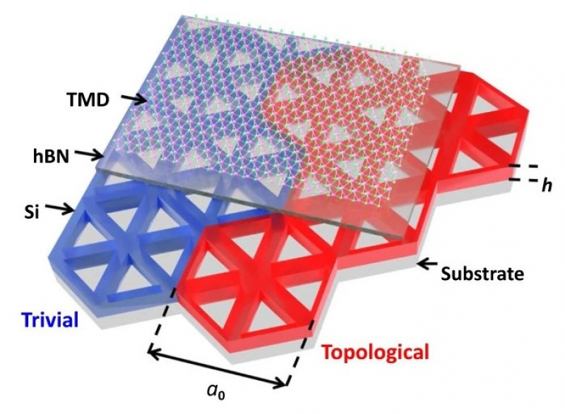
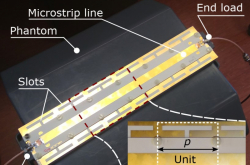
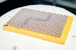
Polariton topological metasurface. Illustration from the article
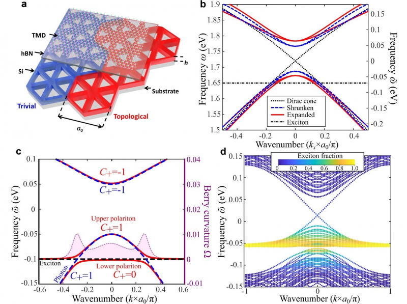
Polariton topological metasurface. Illustration from the article
“Electricity in contact with 2D materials can affect the concentration of carriers in 2D semiconductors more efficiently than when using 3D semiconductors. The reason behind it is that they have fewer carriers and their number can be changed more easily. This has a huge effect on their conducting properties and exciton response. Basically, we can turn excitons off – and polaritons, too – with the help of external voltage sources and thus obtain an electro-optical device, the properties of which we can control. This technology holds great promises, and I believe that it will be an actively studied field in the near future,” concludes Anton Samusev.
Reference: Mengyao Li, Ivan Sinev, Fedor Benimetskiy, Tatyana Ivanova, Ekaterina Khestanova, Svetlana Kiriushechkina, Anton Vakulenko, Sriram Guddala, Maurice Skolnick, Vinod M. Menon, Dmitry Krizhanovskii, Andrea Alù, Anton Samusev & Alexander B. Khanikaev, «Experimental observation of topological Z2 exciton-polaritons in transition metal dichalcogenide monolayers», Nature Communications 2021.