What is the "perovskite revolution", and what were its consequences?
Some hundred years ago perovskite was known only as a rare natural material — calcium titanate (TiCaO3). It was first discovered in Ural Mountains, Russia, and was named after count Lev Perovsky (the perovskites' general formula was called the Perovskit structure). Yet, the new breakthrough in studying a similar material with slightly different components happened only several years ago. This time, it had to do with a new hybrid organic-inorganic material MAPbI3.
In 2013, the Science journal included new hybrid perovskites into the list of breakthrough technologies as promising elements for solar cells. At the same time, scientists discovered that their efficiency output in photovoltaics and LEDs is comparable to that of best traditional semiconductors like silicon or gallium arsenide. Perovskites have one more advantage: they are easier to produce and can be applied on any flexible base — from a sheet of paper of polymer film to fabric.
 ABX3 perovskite structure
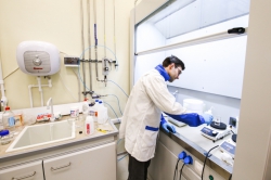
The unique properties of perovskites will be researched in St. Petersburg at ITMO's new laboratory, which is being created as part of the grant won by its scientists in collaboration with the University of Texas at Dallas. Professor Anvar Zakhidov will be the one to represent the American university in this project. It was he who proposed introducing different nanostructures into optoelectric devices so as to increase their efficiency. Also, his laboratory is amongst the few in the world that has the necessary materials for their research. These materials, as well as Mr. Zakhidov's ideas in combination with ITMO's advanced optical equipment will become the basis of this collaboration.
ITMO.NEWS asked the project's head — senior researcher Sergei Makarov from the Department of Nano-Photonics and Metamaterials, and professor Anvar Zakhidov, who came to Saint Petersburg to speak at the kick-off workshop on the project, about the new laboratory, the first results of collaboration and their desired goals.
You started the collaboration in the beginning of 2016, and by last September you've already won the grant. How did the collaboration start and what are its current results?
Anvar Zakhidov: In February, 2016, I came to ITMO University with a big report on perovskites, and Pavel Belov's team got interested in it. Then, in March, Sergei Makarov visited me at my laboratory in the Texas University in Dallas, and we began working on the initial idea of combining nanoparticles and perovskites. We got good results, so soon after Sergei proposed to write a new project, this time for a grant. Even though I had other projects, I agreed. The subject proved to be really interesting. Our first results were already convincing, so we won the grant competition. All that time we were already actively working on our project, as the research itself enticed us much more than the idea of winning.
Sergei Makarov: At the beginning of 2016, we understood that we have common interests, and our research overlaps in many areas. I've been studying nanophotonics for a long time, and Anvar did research on new materials and their use in optoelectronic devices. So, we understood that the state of modern science and technology allows to combine these fields (hybrid perovskites, for instance), i.e. combine new hybrid materials and the new concepts of nanophotonics, so as to create new devices on this basis. Improved solar cells, new lasers, optical sensors, LEDs — this will all be possible thanks to the new approach. We use nanoparticles that allow controlling light on nano scale and making LEDs brighter, lasers — more intensive, and solar cells more effective — simply put, increase the efficiency of all optoelectronic devices based on new materials.
Anvar Zakhidov: As of now, we progress quite fast. In November-December, we understood how great our nanoimprinted perovskite structures are for amplifying light interaction. I'd like to note that they were created at the Texas University, and then brought to ITMO, where we studied these structures and observed an interesting effect — great amplification of non-linear luminescence. We've made the necessary calculations (this was Yuri Kivshar's idea, who came to ITMO from Australia at that time), concentrated on analyzing the results and quickly wrote a good article. I am very glad that our work on the grant began with such a promising science result — the more so we've already made a good publication of it.
They say the laboratory that is being created in St. Petersburg is unique for Russia. Why is that?
Anvar Zahidov: We'll be building this laboratory gradually, in two stages. At first, we will collaborate with the Laboratory of Organic Electronics and Photovoltaics, which is also being created at ITMO University. We will work together with this center and its heads — Victoria Jeltova and Dmitry Parashyk, who are creating a multipurpose base for flexible organic and printed electronics; we will add hybrid perovskites, as well as other hybrid organic-inorganic materials, carbon nanotubes and resonant nanoparticles to their work. ITMO's students will create prototypes of different flexible electronic devices at the laboratory: LEDs, sensors, energy converters, light sources and optical sensors. This work will be conducted on a new multipurpose unit that we'll buy as part of the grant. Yet, the "final" laboratory we aspire to have — "Laboratory of Hybrid Nanophotonics and Optoelectronic", will be built separately, in three year's time. We'll also create small groups for supporting innovations. For instance, we plan to invite Professor Aldo di Carlo from Rome for creating an innovation's center for solar cells.
 ITMO University. Anvar Zakhidov, Sergei Makarov and Aldi di Carlo
Sergei Makarov: In future, we'll stop using regular inorganic semiconductors that are created using complex sputtering techniques, high-temperature processes, vacuum cameras, and so on. We'll be using thin liquid films instead, which will greatly reduce manufacturing costs — as their chemistry is much cheaper than vacuum cameras where one has to sputter ideal layers while adjusting them to each other. In our case, we "mix" the material based on perovskites and "pour" it on the electrode's surface in a thin layer using the so-called "spin-coaters". This does not call for vacuum conditions, expensive materials or semi-conductor technology, and can be used on flexible bases.
In what time do you hope to get the first practical results?
Sergei Makarov: The laboratory will be created during the first year, and completed in three years. During this time, we plan to gather a team of about 15 people, then contract foreign specialists on a full-time basis — we have the necessary funds for it. As of now, our task is to gather a highly qualified team which will continue to work here even after the end of the grant, win new grants, publish articles, get patents and so on.
Anvar Zahidov: During the next three years, we have to get major results and complete the main part of our project. Then, we'll be able to prolong the project for some two years, which is a common practice for those who get such grants. During this period, we'll accomplish a lot: create a laboratory, work together with an engineering center and other teams, bring the project to an international level, then prolong it again and start working on the greater tasks, or dream tasks, as I call them.
What these "dream tasks"are? Please tell us.
Anvar Zahidov: You know the simple lasers that we can carry in a pocket and use as pointers? You press the button, and the battery's electricity becomes light in solid-body diodes. This is called a diode-pumped laser. One of our dreams is to create a diode-pumped laser based on a hybrid perovskite material, which will be very thin and flexible. It will be brighter, it will have different colors, and it will be a lot more effective in every respect. What is more, we will make it flexible or even pliant, like rubber. For instance, it can be in the form of a napkin, or a sturdy piece of cloth. It can even be like a thin rope that you wind around a finger, and it produces light. The application field of such devices is extremely wide. We can make fabrics containing many lasers. We can use lasers to treat and diagnose illnesses, or diagnose the presence of toxic materials, as such lasers are very sensible. And that are only the simplest of applications. The more interesting ones would be photonic chips, or photonic integrated circuits, compatible with silicon CMOS chips. Such chips can become base for new computers and memory devices.
 Nanoimprinted perovskite structure. Diagram
Another big dream that the whole world tries to achieve is the polarton laser, which is based on the new concept of Bose-Einstein condensate. As of now, such lasers are produced at extremely low temperatures and are based on periodic quantum wells created using a very complex and expensive technology; we want to obtain them by simple methods using perovskites with a special nanostructure, which properties have not still been researched enough. We hope those will be able to work at room temperature.
What will be their application?
Anvar Zahidov: Same as in regular lasers. Yet, polaritons can have new interesting applications, as they can propagate with frequencies of teraherz range. Everyone wants teraherzs. Why? They are waves of sub-millimeter frequency that can pass through human bodies, through objects. They can even pass through walls. This might let one see through walls and tell who's there and what exactly he's doing.
This dream is still far from being possible, as there are no such light sources yet. Still, I can say that ITMO has a very strong team, many competent specialists in photonics and optics, and they have been working on this idea for a long time. They have great groundwork in nanophotonics, but they never had the necessary materials until now. We brought the necessary materials, and as we can use them in nanostructures for creating a polariton perovskite laser, we might as well succeed in this field. We sharea dream, and we are ready to work hard to accomplish it.