Problem
In order to examine an object using a regular optical microscope, visual light is focused using special lenses. However, if the object is less than a wavelength in size, it cannot be observed in detail. This is what is called the diffraction limit. The explanation for this phenomenon is such: the electromagnetic field that carries information about the object with a spatial resolution of less than the size of a wavelength is localized near the object, in the near field, and cannot be examined from afar. There are several technologies today capable of overcoming this limit - for instance, near-field optical microscopy. In that case, the electromagnetic field of the object is measured in near field by using a special probe that can interact with the localized electromagnetic field and disperse it into the area where it can be registered by common detectors.
Still, most optical microscopy methods have serious issues with visualizing nanoscale objects in a broad spectral band. The problem is that for different wavelengths - white light, for instance - the lenses refract light differently, which means that the resulting image is distorted. Near-field optical microscopy has another issue: due to the low efficiency of interaction between the localized field and the probe, a more intense light is needed to attain sufficient signal strength. What is more, only a small part of the emission reaches the object, and the rest is dispersed or absorbed, which can damage both the probe and the object. This is why in order to get information about an object with a subwavelength resolution in a broad spectrum; researchers often spend hours scanning at different wavelengths until they cover the whole spectrum.
Researchers from ITMO University solved this problem by using the “nanobulb”, as they call it, - a miniature light source based on a silicon-and-gold nanoparticle. Its main characteristic is that it emits light in an immensely wide wavelength band: from 400 to 1,000 nm. A single nanobulb can register and analyze the optical response of all kinds of subwavelength nanostructures in the whole visible spectrum at the same time. This increases the efficiency and speed of microscopy by several times.
How it works
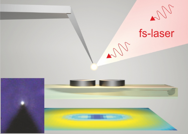
To create the nanobulb, scientists from the Department of Nanophotonics and Metamaterials printed a silicon-and-gold nanoparticle. To make it emit light, i.e. emit photons, it is lit with a femtosecond IR laser. Thanks to this energy, electrons first attain higher energy levels, and then “slide” towards the bottom of silicon’s conduction band, emitting photons on different wavelengths.
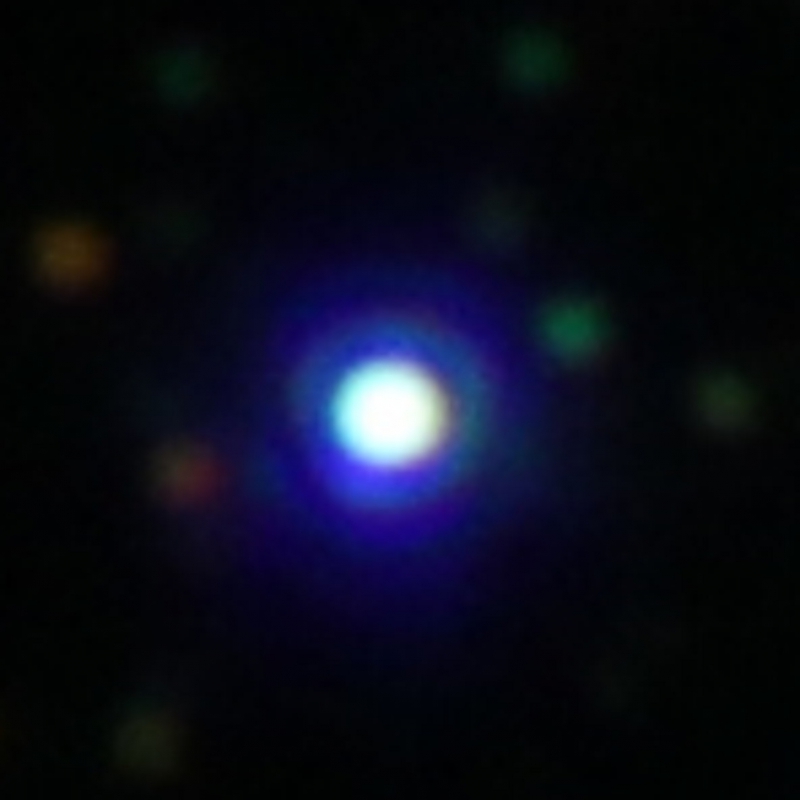
“Silicon, being a nondirect-gap semiconductor, is a poor material for generating emission. In other words, if you light it with a laser, it will absorb maybe a million photons and emit just one. Yet, it is very cheap - you can literally make it from sand. This is why humanity aspires to find as many applications for it as possible: in photovoltaics, microelectronics, and other fields. We have found a most unexpected application, using its main “drawback” – its indirect band-gap – to create a nanosize source of white light that can emit photons of energy 3.4 to 1.1 eV,” - says Sergei Makarov, senior research associate at the Department of Nanophotonics and Metamaterials.
Ivan Sinev, PhD student at the Department, adds that there are two factors that contribute to the nanobulb’s unique properties. Firstly, the laser pumping occurs through very powerful, short impulses that provide for the generation of white light in silicon without destroying it with heat. Secondly, the gold that is added to silicon during the particle creation stage makes the radiance a lot more intensive. Thus, gold increases the light absorption and has an effect on the efficiency of photogeneration of electrons to the higher energy level and their radiative recombination.
“What is more, at the boundary of these two materials, gold and silicon, interfaces emerge that provide for an even better radiative recombination of electrons. Lots of physical mechanisms that we are yet to research are at work here, so there’s a lot of theoretical work that we will have to do to improve our nanobulb, including creating an emittance model,” comments Ivan Sinev.
He notes that another positive feature of the nanobulb is that it uses and IR-band laser to generate visible light. This means that extra “noise” in the optical signal can be removed by way of filtering the dissipated IR light, which improves the effectiveness with which the actual signal is registered.
According to the scientists, this amazing effect was discovered unintentionally as they experimented with laser printing of silicon-and-gold nanoparticles and testing their nonlinear optical properties. Such spherical particles are created by applying a laser to double-layer film. Nanoparticles are printed using laser-printing at the Department of Nanophotonics and Metamaterials since 2015.
“At first, we were just optimizing laser printing of particles that consist of gold and silicon. We aspired to make a common IR-to-ultraviolet or -green converter from each nanoparticle using the popular harmonic generation method, i.e. emission frequency doubling or tripling by means of nonlinear effects. When we started to measure the emission, we saw that we’ve succeeded, but how could we do even better? We decided to amplify the laser radiation, and it turned out that at a higher output the particle changes its color and turns into a “nanobulb” - a bright source of white light. We spent almost a year studying ways to control it and its possible applications. Yuri Kivshar helped us a lot with preparing for the publication,” - explains Sergei Makarov.
Possible uses
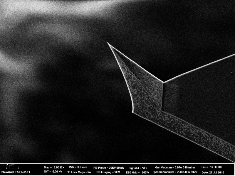
At the suggestion of Anton Samusev, research associate at ITMO University, the nanobulb was placed on a common probe of an atomic-force microscope using a method developed by Ivan Mukhin and Filipp Komissarenko at the Department of Nanophotonics and Metamaterials. The probe allows bringing the source of visible light immediately near the test subject, which greatly amplifies the interaction of the near fields. The signal from this nanoparticle’s emission is registered and separated on a spectrum using a regular spectrometer. Thus, a nanobulb may be integrated into standard microscopic equipment; in other words, it can be attached to any probe and used to record its signals with regular photodetectors – all while receiving information on a nanoobjects’s near-field in the entire visible spectrum band. This means that silicon-gold nanoparticles make microscopy more flexible and cheaper.
“We are also developing an idea of using the nanobulb as a nanolaser. If we place such a particle into a resonator capable of changing the wave’s operating length, we can end up with a tunable laser, one that can function at any set wavelength in the visible spectrum. Besides, the nanobulb may also see use in biology for purposes such as “illuminating” cells and detecting substances that are sensitive to particular wavelengths,” – adds Sinev.
A patent for the nanobulb has already been applied for; in the meantime, the scientists will continue researching its fundamental qualities and possible applications.
Reference: Nanoscale Generation of White Light for Ultrabroadband Nanospectroscopy, S. V. Makarov*, I. S. Sinev, V. A. Milichko, F. E. Komissarenko, D. A. Zuev, E. V. Ushakova, I. S. Mukhin, Y. F. Yu, A. I. Kuznetsov, P. A. Belov, I. V. Iorsh, A. N. Poddubny, A. K. Samusev, and Yu. S. Kivshar, Nano Letters, 2017.