Most materials can be classed as either conductors or insulators: they either conduct the electric current, or they don’t. But there are some that do conduct electricity but only at the thin level of the surface. These materials are known as topological insulators. Their most unusual property is that the current they transmit is resistant to all admixtures and possible defects of the material and “runs” without any losses. This unique property is called a topologically protected edge state.
Topological insulators that would transmit not the electrical current but “protected” electromagnetic waves, will change the development of optical technologies. In modern optical fiber and optical waveguides, the signal mostly propagates in straight lines, scattering in case of any inflections or defects. But if the waveguide is made from a material that supports topologically protected edge states, the light could circumvent the obstacles and propagate without any losses whatever the defects it meets on its way.
Past research in this field showed that under certain conditions, photonic crystals made of ferrite cores can serve as electromagnetic analogs of classical topological insulators (ferrites are magnetic materials made from iron oxides and other metallic elements). But experimental installations with ferrite rods proved to be cumbersome, amounting to several meters in length. Moreover, they only allow for creating topologically protected edge states in the microwave frequency band. In the optical frequency band of visible and near-infrared light, magnetic materials demonstrate but a very weak response.

A new solution for the development of topologically protected edge states in the optical band has been proposed by Alexander Khanikaev, a professor at the City University of New York, the US. The scientist was the first to suggest that topological edge states can be created within the framework of metamaterials. Synthetic compounds with unique electromagnetic properties, they can be used for imitating the properties of electrons in solids, such as the spin (an intrinsic magnetic moment of an electron) and the synthetic fields that act upon them. Moreover, it’s possible to create a metamaterial in which the distance between elements would be much smaller than the length of the wave of a band needed. This wasn’t feasible with magnetic photonic crystals. Thus, metamaterial-based devices can be not only functional but also fairly compact.
The viability of Alexander Khanikaev’s concept was confirmed by an international research group of physicists from Russia, the US and Australia, who conducted a range of experiments at ITMO University. In the first trials, topologically protected edge states were created in a metamaterial that was metal-based. But the latter is unsuitable to work at the optical band frequency because of their considerable light absorption. That’s why in their next experiment, the scientists switched to a dielectric metamaterial, or metasurface consisting of one layer of synthetic structure.
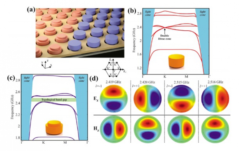
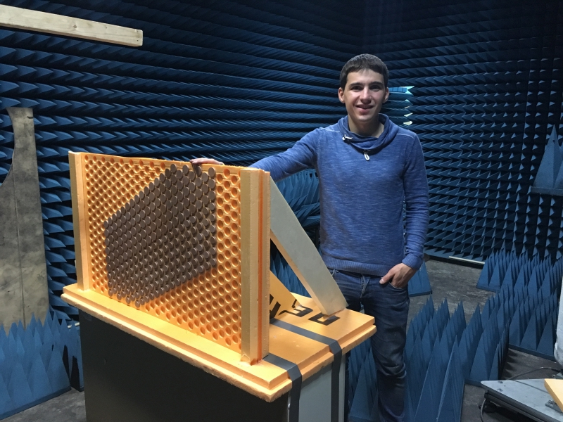
The metasurface comprised a foundation onto which the scientists attached meta-atoms made of ceramic disks. These were arranged in a strict order so that the distance between them would be smaller than a visible-light wavelength. Although the meta-atoms were made in a similar way, they had a different orientation in the final structure: upward in one part, downward in the other. It was at the domain wall, i.e. the border between these two parts, that topologically protected edge states were being created.

Because the researchers only aimed to corroborate the presence of topological edge states on dielectric metasurfaces, the experiments that they conducted were not in the optical frequency band, as it would have required working with elements at the nanoscale. Instead, they opted for a simpler approach, testing the concept in the microwave frequency band. In the end, their hypothesis proved true: the excitation of an electromagnetic wave on the metasurface’s domain wall did cause an edge state to occur. The physicists also demonstrated that the edge state would occur even if the domain wall wasn’t arranged in a straight line but in a zigzag. Used in the optical band, such a structure can provide a foundation for “protected” optical devices.
“We managed to show that you could create a dielectric metasurface that would support topologically protected edge states,” explains Alexey Slobozhanyuk, the lead researcher of the project and a research associate at ITMO University’s Faculty of Physics and Engineering. “Drawing on these findings, we have already come up with a new experiment with meta-atoms of a simpler form that would be easier to reproduce at the nanoscale. This will give way to the development of next-gen optical devices supporting protected edge states in the optical frequency band.”
Topological photonic states open up new possibilities for the management of electromagnetic waves.

“The very opportunity of imitating the phenomena previously considered exclusive to electronic solid-state systems shows great potential for the development of the photonics of metamaterials with synthesized degrees of freedom,” notes Alexander Khanikaev, the head of the project. “Our work experimentally shows that the pseudo-spin wave allows for manipulating the direction of the excitation and propagation of an edge state in metamaterials. In other words, it proves to be not only protected but also controllable. By upscaling our structure to make it work in the near infrared frequency band of optical telecommunications, topological states can become the ideal candidate for a variety of applications in integrated photonics.”
Also participating in the research project were the scientists from the City University of New York and the University of Texas at Austin, the US, as well as from the Australian National University.


