In recent years, physicists from all around the world have started to pay more attention to the topological phase of matter and topological phase shifts. In 2016, a Nobel Prize was awarded for an associated research. Topological shifts offer an opportunity to substantially change the properties of some materials that are used in electronics. While studying the properties of the topological phase of matter, scientists discovered new materials with unique properties that are called topological insulators.
“In nature, there are insulators that don’t conduct electricity, and conductors that do, as well as semiconductors that are of a transitional class,” explains Maxim Gorlach, a co-author of the research and a member of ITMO’s Faculty of Physics and Engineering. “What makes topological insulators interesting is that they are in fact typical insulators, but can conduct electricity through their surface or edges. They were first observed during a study on the physics of the Quantum Hall effect, when electricity was passed through a sample and voltage that took quantized values emerged perpendicularly to the current’s direction. Then it turned out that the quantization takes place despite any impurities or defects of a sample. Later, it was proved that this is how the topological nature of the Quantum Hall effect manifests. And scientists started thinking about the possibility of creating a system that is insensitive to defects and damages in photonics.”
Soon, a counterpart of the Quantum Hall effect was created in the field of photonics, as well. Scientists understood that if they were to create a structure made of ferrite rods, photons would also propagate along its edges without getting inside. This makes it possible to create an optical data transmission line that won’t be affected by damages that can easily cripple a common fiber-optic cable.
In 2017, scientists discovered a new class of topological systems, high-order topological insulators. These materials are characterized by states that can localize themselves along the parts of structures with a dimension that’s less than the dimension of the whole system by a factor of two and more.

“For example, if it’s a cube we’re talking about, then electromagnetic waves in traditional topological insulators propagate along its surface, while high-order topological insulators offer photons an opportunity to “travel” along the cube’s edges or get localized on its corners,” says Dmitry Zhirihin, another co-author of the research and a PhD student at ITMO University.
At the time of the beginning of the research, there were only several theoretical models of hi-order topological insulators that had ever been demonstrated. One of them was a surface that had a structure consisting of hexagonal cells, each containing three elements. Such systems are named kagome lattice after a traditional Japanese woven bamboo pattern. Under specific conditions, the electromagnetic waves can not only propagate along their edges but also focus the field strictly on the corners of the system, which is called topological corner states.
It was these states that a team of scientists led by Alexander Khanikaev, a professor at the City College of New York, wanted to study.
“If we create a structure made of such triangles, then, at specific conditions when the distance between the elements inside the cell is greater than the distance between the nearest elements in two adjacent cells, localized states of an electromagnetic field emerge at all corners of a structure,” explains Dmitry Zhirihin. “These theoretical ideas hadn’t been proved by experiment, and that was our initial task: to study such a kagome lattice and find high-order topological states.”
An unexpected result
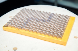
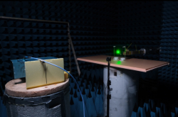
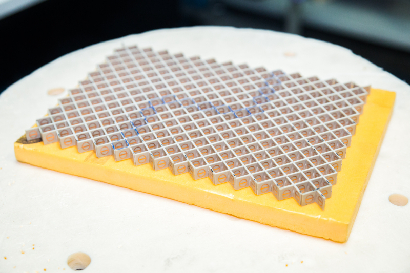
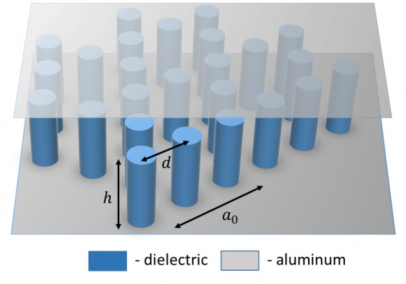
The experiment went as planned: the scientists created a dielectric structure consisting of ceramic cylindrical resonators located in the corners of a kagome lattice. They studied the structure in the microwave band by near electromagnetic field scanning. By experimenting with the distance between cylinders within an elementary cell, the scientists succeeded in observing the previously described effect: at specific frequencies, a topological state of an electromagnetic field emerged at the three cylinders at the edges of the triangular system. It seemed that it should’ve been the end of the experiment: the high-order topological states in photonic kagome lattices were experimentally shown for the first time. Nevertheless, the physicists succeeded in discovering another effect that had never been described before.
“In the course of our work, we’ve found a completely new state, and this is really unusual,” continues Dmitry Zhirihin. “In electromagnetics, we usually work on some theoretical idea, then conduct an experiment to prove it. This time, we observed a new phenomenon during an experiment, and then described it theoretically.”
At a specific frequency one could see that not only the three cylinders located at the corners of a triangular system give a response but also the closest cylinders from each of the triangle’s sides.
“We developed a theoretical model that can be used to describe this additional states with the character of the rod’s interaction, namely their long-range interaction,” explains Maxim Gorlach. “Before, scientists usually used a model of strong interaction for the topological systems, meaning they focused on the interaction of the elements that are closest to each other. Hence, they predicted only one corner state at one specific frequency. Still, it’s obvious that electromagnetic interactions are long-range, meaning that all elements in electromagnetic systems interact with each other. The question is how strong their interaction is. In our system, we deal with propagating waves, therefore we can see the effect of the interaction of the neighboring elements that are far from each other and observe a new topological state that has never been described before.”
Future prospects
Despite the fact that the research can be called a fundamental one, it also has application prospects. The structures used in the experiment can be scaled and used for data transfer and processing, in new optical chips and other microelectronic devices.
“Our work’s main practical significance is that you can control the electromagnetic field on a smaller scale, for example localize it in a very small area (for example at the corner of a structure or at three corners at the same time). In future, this can be applied in optical chips, optical computers, various communications where you will have to control near fields on nanoscale. At the same time, when such devices will be designed, you will have the opportunity to switch between a structure’s states: from the state when the field runs along the edge to the one when it’s focused at a corner,” concludes Alexander Khanikaev.