Microfluidic devices are chips with various micro- and nanostructures (channels, reservoirs, and coils) located on their surface. In their work, scientists add liquids to these chips, allowing these substances to spread inside the microstructures. This way, microelements allow researchers to manage the flow of the liquids – store them, separate them, or mix them – in order to study their properties.
Such chips have various applications: in biomedical testing, the analysis and detection of harmful molecules, and the synthesis of metal-organic frameworks (MOFs) – porous crystalline materials in which the atoms of transition metals are surrounded by ligands (chains of organic molecules). MOFs are also used in different fields, for instance, for air and water purification.
Read also:
ITMO Scientists Suggest Efficient Microfluidic Synthesis for Metal-Organic Frameworks
ITMO Researchers Develop Lab-on-Chip Hardware for Detection of Substance Traces in Media
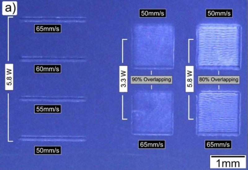
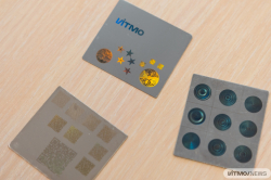
Microfluidic elements and parameters for their fabrication by CO2-laser writing on glass. Image courtesy of Anastasiia Bondarenko
Microfluidic chips can be produced from different materials, but the most promising one is silica glass. According to researchers from ITMO, apart from its outstanding optical properties, this material is resistant to thermal and chemical damage, while also not absorbing elements of analyzed materials. This makes such chips reusable for multiple experiments.
In order to produce microfluidic chips, their basic elements have to be prepared first. All the existing methods (e-beam lithography, gray-scale lithography, and magnetic neutral loop discharge) are time-consuming, expensive, and not energy efficient. Moreover, if researchers need to change the geometry of a chip produced in one of these ways, they would need to create a whole new template for the microstructure.
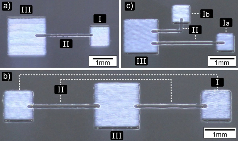
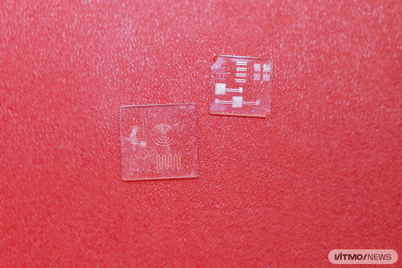
Open surface microfluidic systems acquired by combining microchannels and microreservoirs. In the image: I – input reservoir, II – microchannel, III – reservoir for liquid collection. Image courtesy of Anastasiia Bondarenko
The method suggested at ITMO
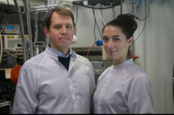
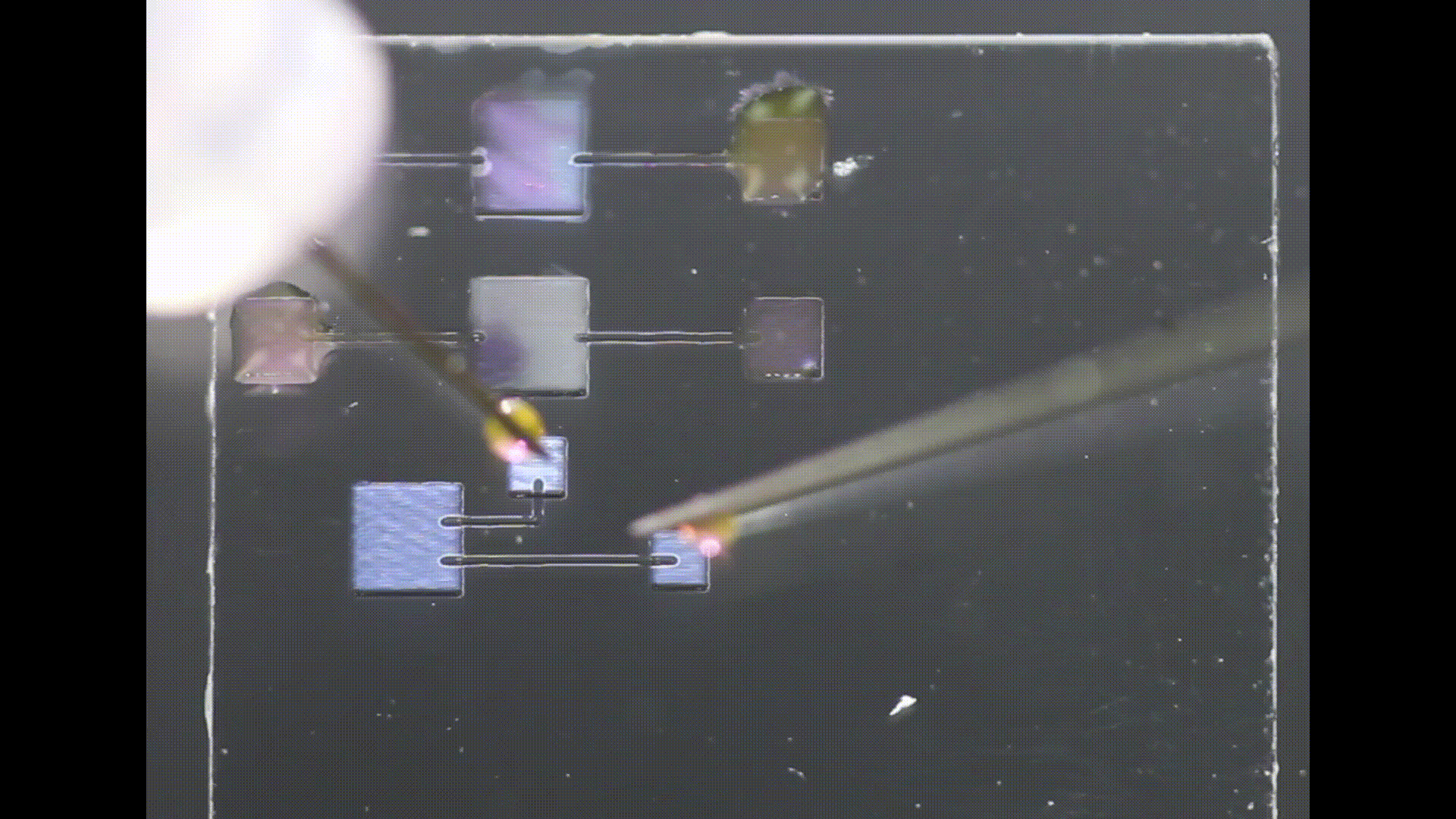
Scientists from ITMO’s Institute of Laser Technologies, in collaboration with the company Laser Center, have developed a new microfluidic chip structuring technology with an affordable CO2 laser. According to Anastasiia Bondarenko, a Master’s student at the institute, the technology is capable of easily fabricating and just as easily adjusting microstructures.
“With our method, you won’t need to go through all the steps required for e-beam lithography, featuring expensive equipment and a vacuum field, if you need to slightly adjust the structure of your chip. You won’t even need a specialized room and a team of professionals. Instead, all you’ll require is a cheap C-Marker laser and one operator – and you’ll be able to fabricate any geometry for various applications,” explains Ms. Bondarenko.
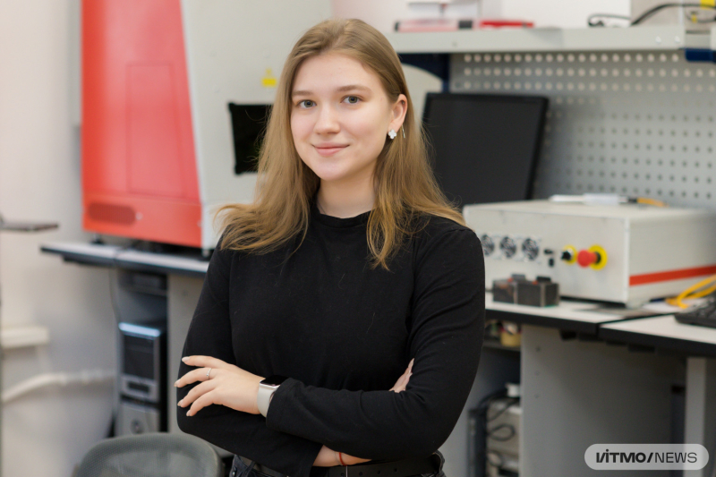
Anastasiia Bondarenko. Photo by Dmitry Grigoryev / ITMO.NEWS
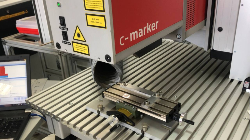
C-Marker laser. Image courtesy of Anastasiia Bondarenko
How it works
In order to prepare silica glass for interaction with a laser, it is first purified in an ultrasound bath with alcohol or distilled water. Then, an operator places the glass into the treatment area and sets the necessary laser power, scanning speed, and pulse frequency. These parameters define the resulting characteristics of the produced microstructures: the channels can be 60-250 micrometers wide with their depth ranging from 0.5 micron to dozens of micrometers.
After that, the operator uses a focused laser beam on the chip’s surface to create the necessary geometrical elements. Thanks to the fact that the glass is good at absorbing laser radiation, it’s possible to remove layers that are mere hundreds of nanometers thick.
As a result, in 10 minutes, a microfluidic system with a low roughness level is produced on the glass surface. This means that up to 100 nanoliters of test liquid can move inside the microstructure with the speed of up to 15 millimeters per second.

Testing microfluidic systems. Filling time: 1.3 seconds.
Testing microfluidic systems. Filling time: 0.9 seconds.
What’s next
The new technology can produce microstructures with different geometries, making the fabricated chips suitable for various tests and experiments. Recently, researchers at ITMO have developed a test system for early diagnostics of inflammatory diseases and oxidative stress.
Read also:
Portable Lab: ITMO Master’s Student On Developing a New Chemiluminescence Sensor
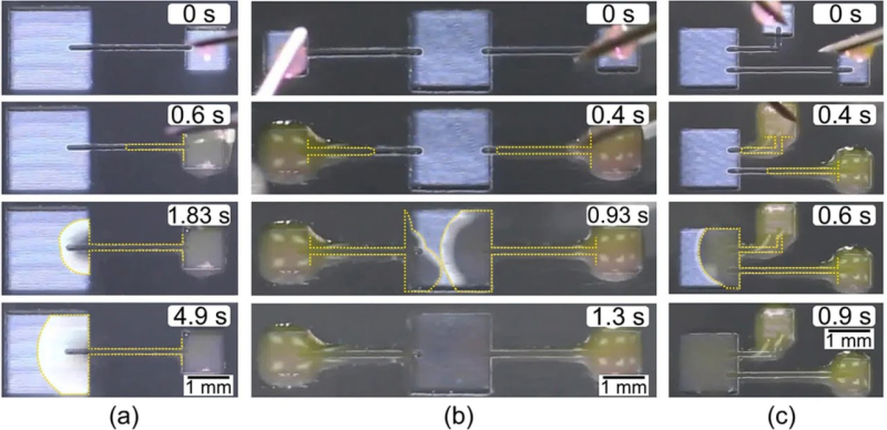
Testing microfluidic systems. Images demonstrating the spread of a solution from the first element down the microchannel towards a reservoir for precipitation. a) filling time of the first system is 4.9 s; b) filling time of the second system is 1.3 s; c) filling time of the third system is 0.9 s. Image courtesy of Anastasiia Bondarenko
“Oxidative stress is at the root of various inflammations, including diabetes, cardiac weakness, diseases of connective tissues, sterility, and even cancer. One of the main causes of stress can be an imbalance of free radicals that generate reactive oxygen species – oxygen metabolites that can include superoxide anion, hydrogen peroxide, nitrogen oxide, as well as hydroxyl and hydroperoxide radicals. We use chemiluminescence to detect hydrogen peroxide in a solution and identify its concentration,” explained Daler Dadadzhanov, a senior researcher at the International Research and Educational Center for Physics of Nanostructures.
Chemiluminescent analysis is made possible with microfluidic chips. For instance, using the chip, researchers can separate the solution into two channels to compare them. The first one will be left untouched, while the solution in the second will be mixed with luminol (a luminescent agent) and H2O2, an oxidizer and catalyst, to track the oxidation of the solution. This reaction will produce energy that will transform into radiation. By analyzing the intensity of this radiation, researchers will be able to detect hydrogen peroxide in a solution, specify its concentration, and diagnose an illness.
This study was supported by a grant for Master’s and PhD students from ITMO’s School of Physics and Engineering.
Reference: A. Bondarenko, A. Ramos-Velazquez, A. Shmalko, R. Zakoldaev. Surface microfluidics elements fabrication by CO2-laser writing on glass: challenges and perspectives (Optical and Quantum Electronics, 2023).