A group of researchers from ITMO University and Herzen State Pedagogical University are working on new sensors operating in the THz frequency range as part of a grant provided by the Russian Scientific Foundation. To create prototypes for such devices, the researchers have to synthesize materials that will have the necessary optical qualities in the THz frequency range. They have managed to do this by making bismuth-based double-layered structures. Their results have been published in Rapid Research Letters. ITMO.NEWS talked to the researchers and learned how they managed to synthesize this new material, why this project is significant and how it is connected to radio astronomy.
Up until very recently, it was hard for scientists and engineers to work with THz radiation. Now, however, more and more opportunities appear to use the radiation of this frequency in various fields of science – from spectroscopy to wireless data transmission.
Currently, researchers are only beginning to discover the THz range, and to use it completely, new accessible and efficient devices need to be created. Thus, there is a demand for a portable supersensitive high-performance detector that could work outside the controlled lab conditions – in a typical space with room temperature.
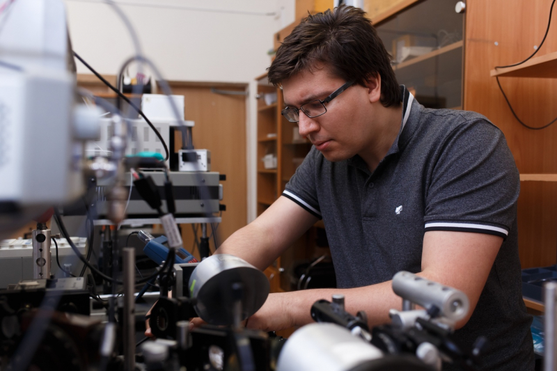
It is exactly this task that scientists from ITMO (School of Photonics and School of Biotechnology and Cryogenic Systems) and Herzen State Pedagogical University are planning to solve. First, however, they needed to find the material they were going to use to create this device.
Hyperbolic medium
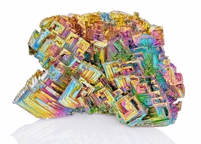
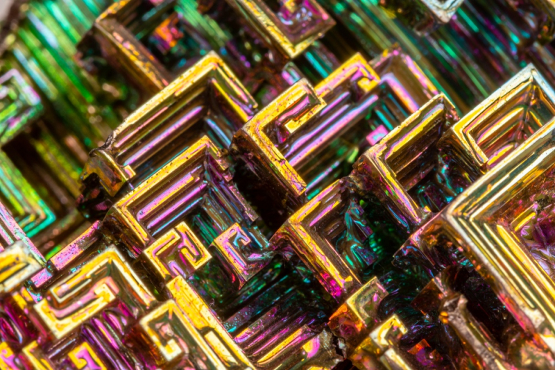
The researchers decided to base their new material on bismuth. Such materials are semimetals with a small overlap between the valence band and the conduction band, which is important for detective devices in the THz frequency range.
“There are three dielectrics, semiconductors and conductors,” says Petr Demchenko, co-author of the paper and engineer at ITMO’s Terahertz Biomedicine laboratory. “They have different widths of the energy gap. In metals which are conductors, the valence and conduction bands overlap. Semiconductors have an energy gap. In semiconductors, this gap is up to 3eV, and in dielectrics it is between 3eV and 5eV which makes it impossible for the electric current to run through it. But there is a class of semimetals between these two that includes stibium, stannum and bismuth. The band overlap in them is small, but it still exists.”
Moreover, bismuth and stibium potentially had another important quality. Previously published theoretical papers suggested that bismuth-based materials could demonstrate properties of a hyperbolic medium in the THz range. This, however, had not been proven experimentally.
“Hyperbolic media are a special class of optical materials,” explains Anton Zaitsev, another co-author of the paper, engineer at ITMO’s Terahertz Biomedicine laboratory. “The main components of the dielectric conductivity in such materials have opposite charges in different directions, which provides for rather unusual effects. For instance, the opportunity to get a negative refractive index, which is impossible in standard optical materials. It means that in a certain frequency range in different directions the material can either be a dielectric unaffected by radiation, or a metal that reflects or absorbs it.”
How to spray bismuth on mica
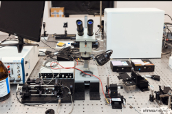
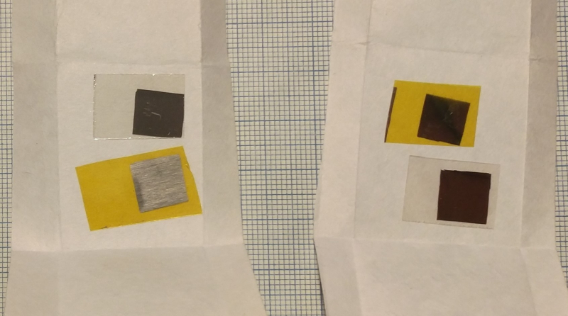
To create these properties in the exact part of the THz frequency range, the scientists decided to grow a bismuth crystalline structure on a mica surface. For that, they chose a method called thermal precipitation or thermal spraying.
“It all happens in a flask with the air pumped out of it,” expounds Petr Demchenko. “The flask has a special tube with a sliding cylinder which grinds the incoming material – in this case, bismuth. Then, particles of bismuth get on the thermal element, a molybdenum boat inlet. We can regulate the layer thickness in the final material by regulating the mass of these particles. The thermal element is heated up to 270 degrees, so that bismuth turns into gas jumping over the liquid state. There is a valve above the thermal element that stays closed until there is enough gas in the flask – then it opens and bismuth comes up where there is a holder with a mica plate that has a patterned metallic mask on it. The gas settles on the plate, which is also heated so that the gas particles don’t all collect in one place but form a crystalline structure. After that, the plate is kept under the temperature of 250 degrees for half an hour. Thanks to this, the structure stabilizes, and we get a thin double-layered structure – the thickness of bismuth is between tens and hundreds of nanometers, and the mica plate is 17 micron. It’s roughly five times thinner than a human hair.”
This method is much easier and cheaper than molecular epitaxy often used to create semiconductor heterostructures. Potentially, it means that the devices based on this new material will be more accessible than analogues made from such heterostructures.
Negative refractive index
The physicists analyzed the optical properties of their acquired materials to prove that the structure does have hyperbolic qualities in the low-pass area of the THz range. After studying the characteristics of pulses going through the materials, the scientists saw that the time latency was negative in comparison with that of radiation passing through the air medium. The length of the time latency depends on the thickness of the bismuth layer.
“During an experiment, we discovered that the radiation going through bismuth and mica starts passing through them faster than it does through air, when we raise the thickness of bismuth,” says Petr Demchenko.
Thus, the material behaves like a hyperbolic medium, specifically in the THz range, which could not be achieved before.
Possible applications
The new material will be used to create a prototype of a portable high performance supersensitive THz detector. It’s planned that the work will resume in July after the break due to restrictions during the pandemic.
However, this is not the only possible application – potentially the material can be used in communication and probing systems, and in biosensorics.

“Our material will make it possible to create a matrix of THz detectors that could be used in airport and railroad station security systems to scan luggage, as well as to diagnose illnesses,” comments Mikhail Khodzitsky, head of the grant project, an associate professor and head of ITMO’s Terahertz Biomedicine laboratory.
The material can also be used to create a masking surface hiding objects from THz radiation, thus making them invisible for THz radars. Finally, it can be used in radio astronomy.
“We often do not clarify that the telescopes used in radio astronomy also work in the THz range, which is exactly the range our experiments operate in,” adds Petr Demchenko. “Black holes, for instance, are studied in this range. To do that, researchers apply semiconductor detectors that are first cooled down to the temperature of liquid helium. Our detector will be able to operate at room temperature.”