Today, perovskites are among the most actively studied materials. The first perovskite known to science was calcium titanate, a mineral discovered in 1839 in the Ural Mountains. For a long time, it was considered a potential material for use in capacitors. In the 1980s, more complex perovskites started to see use in high-temperature superconductors. But in the early 21st century, they were “rediscovered” as a valuable raw material for photonics.
The so-called halide perovskites hold great potential for use in optical systems. Lasers made using these materials can produce extremely spectrally narrow and bright light. Perovskites are also efficient at absorbing light energy, making them useful in the development of solar power technologies. Eight years ago, Science featured the use of this material in photovoltaics as one of 2013’s top scientific breakthroughs.
But there are still a number of challenges to be overcome before perovskites can see widespread commercial use. One such challenge is to find a cheap, effective way of moulding them into specific shapes.
“You could liken it to jewelry: it’s not just about the quality of a diamond, but the way it’s cut, too,” explains Sergey Makarov, dean of the Faculty of Photonics at ITMO University. “You need to treat the stone, giving it a new shape while preserving its qualities. It’s the same with perovskites – they need to be processed before being turned into, say, a microlens or any other optical element. But we also have to make sure not to diminish its functional qualities, most of all its optical transparency and luminescence.”
Sergey Makarov
Issues with existing methods
Today, scientists know of a few ways to process semiconductor materials. These methods make it possible to carve, stamp, or etch a specific pattern onto a sample surface or to endow the microcrystal with a specific shape. But these methods don’t work well with micro- and nano-scale perovskite particles.
“For instance, one of the most accurate nanolithography methods is lithography with a focused ion beam,” says Sergey Makarov. “In that case, a stream of ions is aimed at the material and used to “shave off” the extra bits. But it doesn’t work with perovskites. The gallium ions used for that purpose damage the crystalline structure and penetrate it. You just end up wasting the material. Even if it looks good after processing, its optical qualities will nevertheless be hopelessly deteriorated.”
The reason is that the gallium ions, having made themselves part of the crystalline structure, begin to absorb light instead of letting it pass through. As a result, such a crystal can no longer be used in a laser. This caused the scientists to experiment with various other perovskite processing methods. Some were productive, but difficult to implement and sometimes resulted in loss of material.
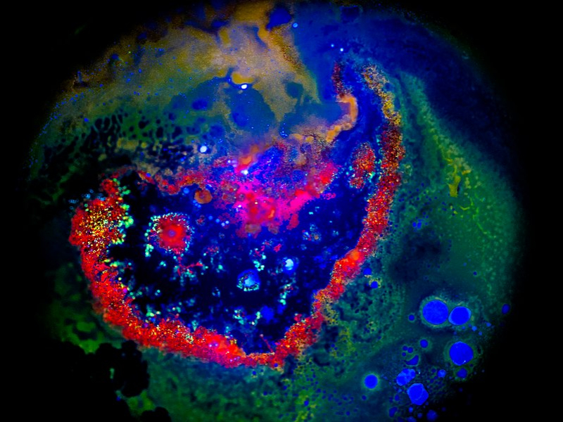
Cube-shaped perovskites. Photo courtesy of the researchers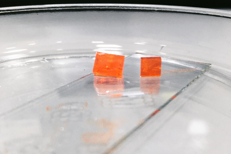
“For instance, there’s multi-stage lithography with the use of photoresistors,” explains Sergey Makarov. “It involves the application of liquid materials onto the sample as protection. But we’re working with microcrystals, which don’t attach very well to a substrate. So when we apply liquid materials, we risk moving them or washing them away completely. We can use nanoimprint lithography, which is when patterns are applied onto crystals using a mould and pressure. But there’s an issue, too, as the pressure may just as well move the microcrystal and end up damaging it.”
Laser processing
An international research team that includes scientists from ITMO University, the Far Eastern Federal University (FEFU), the Image Processing Systems Institute of RAS, and Tokai University (Japan) have suggested another way of moulding monocrystals into the proper shape.
“In our previous research, we worked with laser ablation of thin film made up of a multitude of perovskite nanocrystals,” recalls Aleksandr Kuchmizhak, a senior researcher at FEFU’s Pacific Quantum Center and the Image Processing Systems Institute, a co-author of the paper. “We demonstrated that lasers can be used to cut the film into microstructures of various shapes. This type of processing also didn’t result in loss of any optical or light-emitting qualities. It was decided to use that research to try a similar method for the processing of single perovskite micro- and nano- crystals.”
Aleksandr Kuchmizhak
To that end, the researchers used ultra-short (femtosecond) laser pulses. Since perovskites have relatively low heat conductivity properties, the scientists were able to laser-etch the necessary parts of the crystal without damaging nearby fragments of its structure. Thus, they were able to cut the monocrystals into lenses and other elements used in optical systems.
“By using the method we developed, we were able to form various optical microstructures – different microlenses, subwave diffraction gratings with a period significantly smaller than the wavelength of optical radiation, etc. But perovskite optical elements can be used not just as passive devices: when there’s a need to deflect a beam or focus it into a diffraction limit, they can also be used as functional elements of more complex active optical devices: microlasers, ultrafast modulators, and other parts of cutting-edge optical chips,” says Alexey Zhizhchenko, a senior researcher at FEFU and the Image Processing Systems Institute, a co-author of the paper.
Alexey Zhizhchenko
This research opens up new opportunities for the creation of high-quality perovskite-based elements for microoptics. It may also help bring about the material’s widespread adoption for use in microchips and other optoelectronic devices.
A.Y. Zhizhchenko, A.B. Cherepakhin, M. Masharin, A. Pushkarev, S.A. Kulinich, A. Porfirev, A.A. Kuchmizhak, S.V. Makarov. Direct Imprinting of Laser Field on Halide Perovskite Single Crystal for Advanced Photonic Applications. Laser & Photonics Reviews, 2021