This year, the international community of optical physicists celebrates the anniversary of a milestone event: 60 years ago, in the middle of May, American physicist Theodor Maiman demonstrated the operation of the first optical quantum generator - a laser. This gave way to a new era in which lasers have become an essential part of our lives.
Sixty years later, an international team of scientists, most of whom are from ITMO University, published a research where they demonstrated experimentally the world’s most compact semiconductor laser that works in the visible range at room temperature. This means that the coherent green light that it produces can be easily registered and even seen by a naked eye using a standard optical microscope.
It’s worth mentioning that the scientists succeeded in conquering the green part of the visible band which was considered problematic for nanolasers.
“In the modern field of light-emitting semiconductors, there is the “green gap” problem,” says Sergey Makarov, principal investigator of the article and professor at the Faculty of Physics and Engineering of ITMO University. “The green gap means that the quantum efficiency of conventional semiconductor materials used for light-emitting diodes falls dramatically in the green part of the spectrum. This problem complicates the development of room temperature nanolasers made of conventional semiconductor materials.”
Material selection
The green gap problem hindered the creation of small green lasers based on metal-dielectric technology which has been successfully used in the creation of subwavelength lasers that work in the infrared (IR) band.
“When people began to try creating such nanolasers in the visible range,” says Sergey Makarov, “they tried to do everything the same way as they did with metal-dielectric IR lasers, where the light could be “shrinked” to the size less than that of a wavelength by means of the excitation of plasmons in the metallic parts. But in the visible range, due to significant losses in most metals, the most of light energy converts into parasitic heat and destroys the nanolaser.”
In order to solve these problems, a team of physicists and chemists from ITMO University and their foreign colleagues from the Australian National University, the Chalmers University of Technology and the University of Texas at Dallas decided to avoid the metal-dielectric designs and develop the fully dielectric concept, so they turned their attention to halide perovskite, which has prospective light-emitting properties due to high quantum efficiency of luminescence in the visible band. What’s more, the physical properties of perovskite allowed the researchers to come up with the laser’s original design.
Two in one
A traditional laser consists of two key elements – an active medium that allows it to generate coherent stimulated emission and an optical resonator that helps confine electromagnetic energy inside for a long time. Perovskite can provide both of these properties: a nanoparticle of a certain shape can act as both the active medium and the efficient resonator.
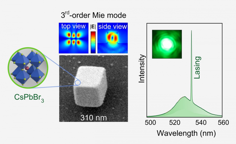
“In order to confine the radiation and amplify it inside the nanoparticle, we use geometric resonances which resonant wavelengths fit an integer number of times from one resonator plane to another, says Kirill Koshelev, one of the article’s authors and a junior research fellow at ITMO University. “This effect is called the geometrical resonance or the Mie resonance, after Gustav Mie who described similar phenomena for spherical particles over a hundred years ago. Perovskite has a cubic crystalline lattice, and if we use chemical synthesis to fabricate the particles, they will naturally obtain a cubic-like shape, which is an optimal shape for a resonator as it has many directions of symmetry and is therefore good at confining energy.”
Chemical synthesis
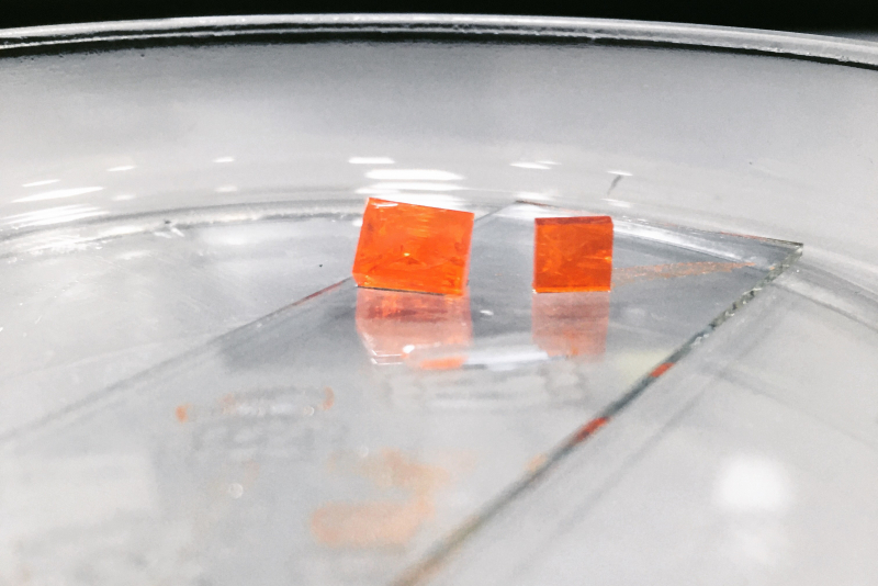
Despite the fact that perovskite has a cubic crystalline lattice and under the right conditions, its particles take on the shape that’s close to that of a cube on their own, producing a nanoparticle of a specific size, form and quality is not easy. You need special conditions.
“Traditionally, cubic perovskite particles were produced with the help of such methods when you first produce spherical particles that then become cubic,” explains Aleksandra Furasova, paper co-author and a junior research fellow at ITMO University. “But that doesn’t help with the tasks of nanophotonics, because they turn out too big. We used a two-stage chemical synthesis: we first produced lead bromide PbBr2, such little embryos of crystals, and then added cesium bromide CsBr to produce perovskite cubes (CsPbBr3). The chemical synthesis methods that were described before didn’t allow us to produce the particles of the size in question, and we needed separate crystals for further research and applications. For this reason, we grew perovskites on special substrates while adjusting the humidity, temperature and the combinations of solvents used.”
But even this method produces particles of different sizes. After the synthesis, it was necessary to use complex theoretical modeling to identify the crystals that were good for the experiment. In the end, it turned out that those were particles of 310 nanometers in size.
How it works
But the crystal by itself is not a laser yet. In order to emit coherent light, one has to excite it or, as they say, “pump” it with energy until a stimulated emission occurs.
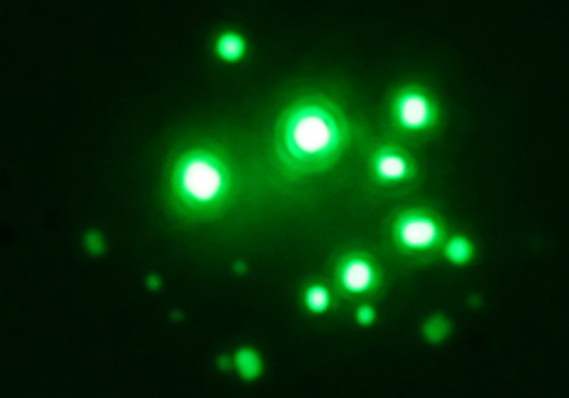
“We used femtosecond laser pulses to pump the nanolasers,” says Ekaterina Tiguntseva, a junior research fellow at ITMO University and one of the article’s co-authors. “We irradiated isolated nanoparticles until we reached the threshold of laser generation at a specific pump intensity. After that, the nanoparticle starts working as a typical laser. We demonstrated that such a nanolaser can operate during at least a million cycles of excitation.”
The uniqueness of the developed nanolaser is not limited to its small size. The novel design of nanoparticles allows for efficient confinement of the stimulated emission energy to provide a high enough amplification of electromagnetic fields for laser generation.
“The idea is that laser generation is a threshold process,” explains Kirill Koshelev, a junior research fellow at ITMO University and one of the article’s co-authors. “i.e. you excite the nanoparticle with a laser pulse, and at a specific “threshold” intensity of the external source, the particle starts to generate laser emission. If you are unable to confine the light inside well enough, there will be no laser emission. In the previous experiments with other materials and systems, but similar ideas, it was shown that you can use Mie resonances of the fourth order or fifth order, meaning resonances where the wavelength of light inside the material fits the resonator volume four or five times times at the frequency of laser generation. We’ve shown that our particle supports a Mie resonance of the third order, which has never been done before. In other words, we can produce a coherent stimulated emission at the conditions when the resonator size is equal to three wavelengths of light inside the material.”
Prospects
Another important thing is that there is no need to apply external pressure or very low temperature for the nanoparticle to work as a laser. All the effects described in the research were produced at a regular atmospheric pressure and room temperature. This makes the technology attractive for specialists who focus on the creation of optical chips, sensors and other devices that use light to transfer and process information, including chips for optical computers.
The benefit of lasers that work in the visible range is that with all other properties being equal, they are smaller than red and infrared sources with the same properties. Thing is, the volume of the small lasers generally has a cubic dependence on the emission’s wavelength, and as the wavelength of green light is three times less than that of infrared light, the limit of miniaturization is a lot greater for green lasers. This is essential for the production of ultracompact components for future optical computer systems.
The article has been published in ACS Nano, one of the leading journals in the associated research field. It’s worth mentioning that it is indexed by Nature Index, a prestigious ranking that shows the level of research institutions with regard to not just the number of high-level articles, but also the contribution to them by authors from universities and institutes. According to this ranking, ITMO University is among Russia’s top three universities in physics, and also holds leading positions in several other categories.
Reference: Tiguntseva E., Koshelev K., Furasova A., Tonkaev P., Mikhailovskii V., Ushakova E.V., Baranov D.G., Shegai T., Zakhidov A.A., Kivshar Y., Makarov S.V. Room-Temperature Lasing from Mie-Resonant Non-Plasmonic Nanoparticles. ACS Nano, 2020/10.1021/acsnano.0c01468