A regular beam of light propagates in a single direction, but the wave can be made to rotate around itself – a phenomenon called a vortex beam. Vortex beams have a singular property, the orbital angular momentum: the phase of the light wave twists in a spiral around the propagation direction.
In photonics, light with various values of orbital angular momentum can be used as different states in information transfer and processing. In optical communications, this means an additional way to encrypt data: several beams with varying “twists” can propagate simultaneously and act as independent communication channels – as shown by ITMO researchers in a previous study. To take such systems further, researchers need compact sources of vortex radiation with preselected properties, such as OAM (orbital angular momentum) devices integrated into photonic chips.
In the long run, such materials can be used to develop various elements of photonic integrated circuits, such as photodetectors and modulators. They can be used in AI, quantum technologies, and sensorics (as a light source to detect toxic gas in the air and analyze biomolecules).
The properties of vortex light can be controlled with various implements such as metasurfaces, nanoantennas, and special gratings in microlasers. Researchers from ITMO’s Laboratory of Hybrid Nanophotonics and Optoelectronics and the Far Eastern Branch of the Russian Academy of Sciences have suggested a simpler method: a new-geometry microlaser from the halide perovskite MAPbBr₃. Unlike with existing methods, the laser’s production doesn’t involve complex multistep lithography. The device is a microdisk with nanopores along its edge, forming a gear-like structure.
Perovskites can generate light when subjected to optical pumping. Thanks to the microdisk shape, the light doesn’t radiate outside but propagates along the edge in a circle. The heterogeneous indents made in a particular order and distance from each other are needed to turn it into a vortex beam and diffuse the waves outside. Thus, the light coming out of various nanopores is assembled into a structure needed to create a vortex beam. By changing the device’s geometry – the disk’s radius or location of nanopores – researchers can manually control the properties of light emitted by the microlaser.
“We’ve been working with perovskite micro- and nanolasers for about nine years and we see great potential in perovskite integrated photonics – that is, in creating miniature optical devices that can be combined on a single chip. Perovskites have a high refractive index and are thus suitable for the creation of nanowaveguides through which light propagates,” says Sergey Makarov, one of the paper’s authors, the head of ITMO’s Laboratory of Hybrid Nanophotonics and Optoelectronics, as well as the university’s new Institute of Photonics.

Sergey Makarov. Credit: Dmitry Grigoryev / ITMO NEWS
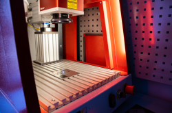
To create the structure, the researchers used a femtosecond laser with very short pulses. Using a spatial light modulator (a device that changes the amplitude or phase of light waves), the researchers formed several laser blots and placed them in a circle. Next, the pattern was turned and transferred onto the perovskite. The result was a regular system of nanopores with a period of about 270-300 nanometers. The most compact microlaser was less than 3 microns in diameter.
“Our unique approach to treating the structure with a femtosecond laser allows us to control the beam not only inside the chip, but also outside it. This property can be useful in systems where light has to leave the photonic chip, pass through space, and land on another element or detector,” shares Alexey Zhizhchenko, the paper’s first author and a senior researcher at the Far Eastern Branch of the Russian Academy of Sciences.
Unlike its predecessors, the method makes it possible to create microlasers directly with a laser. At the same time, it was important to select the structure’s geometry: one device had to contain small holes and a microring that is significantly larger in size.
Next, the researchers are planning to study ways to control the emerging laser radiation in more detail, as well as explore microlaser applications in telecom.
This study was supported by the Russian Science Foundation (grant No. 24−79−10271), the Ministry of Science and Higher Education, and the federal program Priority 2030.