Today the development of electronics, which have revolutionized the previous century, is entering a new stage. In some areas, its capabilities are reaching a fundamental limit, pushing scientists to seek out new technological solutions.
In the past, the development of electronics occurred in several stages: from the understanding of the basic principles and creation of the primary components, semiconductor diodes and transistors to the appearance of devices with a large-scale integration, like microchips and processing units. 30 years ago, it was nearly impossible to imagine that humanity would possess the technological capabilities to produce powerful and compact electronics for personal everyday use on an industrial level.
The capabilities of modern electronics are largely owed to breakthrough discoveries of new materials and large-scale integration technologies. The latter, however, is now a cause of limitations in the advance of electronic devices. The reduction in size and the extremely high density of processing unit components are causing a number of issues that can’t be solved using today’s technology.
New requirements that are posed towards information systems (further reduction in size of wearable tech, increase in operation speed and efficiency) are making it necessary to use photons, not electrons, as data carriers.

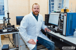
“One of the biggest trends in science today is to move away from electronic data processing towards optical data processing. This change solves at least three issues. First of all, it reduces the cost of technological production – after all, manufacturing nanophotonics devices or their components doesn’t call for massive machines or expensive, environmentally unsafe elements. Secondly, there’s no faster way to transfer data than with light. No electronics are even comparable. Thirdly, all electronics are susceptible to breakdown under the effects of, say, heat. This problem was recently brought up in an issue of Science [Vol. 458, Issue 6366, pp. 998] in regards to the possible ways to control probes sent to study the surface of Venus. It’s an extremely hot planet, and so none of the transistors we have today would work there. So what materials and data analysis methods do we need to overcome this? This is where nanophotonics comes in; the primary materials there these days are heat-proof, nonorganic or hybrid metal-organic structure,” – explains Valentin Milichko, research fellow at the Department of Nanophotonics and Metamaterials.
Today the creation of new photonic nanodevices is one of the most important areas of research. Solutions to a variety of fundamental and technological challenges are being worked on intensely, including as part of national programs in the US, Europe, Russia and China.
Joint project
A series of studies as part of the project “Hybrid Photonic Nanodevices” are being carried out by scientists from ITMO University’s Department of Nanophotonics and Metamaterials. The project, which the Russian scientists are working on in collaboration with their colleagues from Institute Jean Lamour (France), has recently won a grant as part of the federal targeted program “Research and development in high-priority areas for development of the Russian science and technology in 2014-2020.”
This international project, which aims to deepen the collaboration between the two countries, will last for three years. On the Russian side, the project is sponsored by the Russian Ministry of Education and Science, and on the French – by the French National Center for Scientific Research (CNRS).
Together, scientists will develop ways of producing new, unprecedented nanostructures and nanocomposites, including hybrid crystalline nanoparticles based on two metals, metal-insulators and metal-organics. In the future, these new nanostructures, once their effectiveness is proven through joint testing, may become a foundation for the creation of hybrid photonic nanodevices.
“An important distinguishing feature of the materials we’re developing is that these nanostructures are, firstly, crystalline and, secondly, consist of several materials. It might be a metal, an insulator, or some organic materials. The methods for producing such materials are quite difficult. These days it’s incredibly difficult to achieve such properties as crystallinity and varied morphology and chemical makeup all at the same time. With this project, we will develop these exact kinds of structures. This has the potential to result in the creation of photonic devices of a higher efficiency, higher response speed and a number of other improvements – like optical switches and nanolasers, i.e. devices based on the principles of optics, not electronics,” – comments Valentin Milichko – “Another task we have to complete as part of the project is to exchange unique experience with our French colleagues.”
Plans
The Institut Jean Lamour is a branch of the National Center for Scientific Research (Centre National de la Recherche Scientifique, CNRS). French specialists are some of the best in Europe in the field of high-definition electron microscopy, which is needed to characterize and study complex hybrid objects made at nano-scale; it lets scientists verify immediately how well-placed the atoms are and whether the crystalline structure is stable, as it determines the optical properties of the final objects. French scientists also have a lot of experience in - and made significant contributions to - the field of cryogenic electron microscopy (this year’s Nobel Prize in Chemistry was awarded for this very method).

Scientists at Institute Jean Lamour can use plasma chemistry and 3D-printing to produce unique nanoobjects that contain several elements of the periodic table (bimetallic nanoparticles). These objects are distinguished by a high degree of crystallinity and unique alloy composition, which is necessary for nanophotonics devices.
Researchers at ITMO University, for their part, have experiences with nanophotonics and non-linear optics, and can carry out a complete optical characterization of the nanoobjects, which will let them prove their properties experimentally and open up possibilities of their later practical applications. In addition, the department’s specialists have already been able to produce a number of crystalline hybrid metal-organic nanoparticles.
As Valentin Milichko points out, this collaboration began six months ago with a partnership proposal from the French researchers. After several meetings, the two scientific teams decided to combine their unique competencies in a joint project dedicated to the development of materials for cutting-edge nanophotonics devices. They’re not starting from scratch, either: the researchers already have produced some impressive results. The French team, for instance, were the first in the world to produce crystalline bimetallic nanoparticles based on copper and silver, resulting in a unique alloy that had never been produced before. ITMO’s research team completed a full optical characterization of these particles and confirmed that they can be potentially used as objects for amplified Raman scattering and for working with molecular luminescent systems.

Researchers from the Department of Nanophotonics and Metamaterials, similarly, were the first to create hybrid crystalline hollow nanoparticles based on metal ions and organic components.
“These objects are hollow crystalline spheres that have no comparable counterparts in the world. We’ve already subjected them to optical characterization and will utilize them in a sequence of experiments together with the French team to prove all of their structural and non-linear-optical properties,” – says Valentin Milichko.
The three-year project will result in a technology for production of new hybrid nanoparticles and the experimental proof of their unique photonic properties. Nevertheless, this collaboration will not end after three years – the scientists plan to continue their work together on several other projects.