Perovskites are a class of materials with a specific crystalline structure. They were first discovered in the first half of the 19th century in the Ural region as a mineral that consisted of calcium, titanium and oxygen atoms. From then on, perovskites were applied in both nonlinear optics and the manufacturing of semiconductors. Now, they are rapidly winning the ground in the fields of solar power industry and photonics: in 2013, research on the use of these materials made it into Science’s top ten breakthroughs, as new organic-inorganic perovskites already pose a competition to silicon and gallium arsenide.
Perovskites can be used to create tiny lasers that are smaller than the size of the lightwave they emit. At the same time, these light sources can be easily adjusted in the visual band, or, to put it simply, their signal can be of different colors. But there’s a price to pay: it’s quite hard to create miniscule perovskite structures, something of tens of nanometers in size. This hinders the active industrial introduction of this material.
“Perovskites are too sensitive to standard nanostructuring procedures,” comments Sergey Makarov, senior researcher from ITMO’s Faculty of Physics and Engineering. “In order to create nanostructures from silicon or gallium arsenide, we use lithographic methods based on gas- or liquid-phase etching. But you can’t do that with perovskites: the reagents are likely to simply degrade the material.”
Laser etching
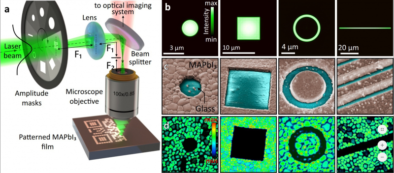
Apart from a high sensitivity to etching reagents, perovskites have another feature: extremely low heat conductivity. Perovskites transfer heat even worse than glass. So, scientists from ITMO University and Far Eastern Federal University (FEFU) proposed a method for processing perovskite with the help of a laser.
“It is very difficult to nanostructurize conventional semiconductors, such as gallium arsenide, using a powerful pulsed laser,” says Sergey Makarov, “The heat is scattered in all directions and all the thin, sharp edges are simply distorted by this heat. It's like if you try to make a miniature tattoo with fine details, but due to paint spreading out under the skin, you will just get an ugly blue spot. Perovskite has poor thermal conductivity, so our patterns turned out very precise and very small."
Researchers from St. Petersburg prepared the material which was then processed at Far Eastern Federal University with the help of a femtosecond laser and a precise positioning system. Scientists from Vladivostok, who are very experienced in nanostructuring, created laser beams with a specific profile.
“With due regard to the structure, chemical composition and other properties of perovskite materials, we proposed a laser processing technology of our own. In order to avoid such harmful effects as overheating, we used ultrashort laser impulses. We chose to use such intensity that the temperature at the spots of material’s evaporation was only 1600C. We succeeded in evenly and precisely removing the perovskite, layer by layer, in the chosen area without sufficient negative effects on the surrounding material. I have to say that this technology offers exquisite printing quality,” says Aleksandr Kuchmizhak, research officer at the NTI Center for Neurotechnology and VR/AR Technologies of Far Eastern Federal University.
Colored solar cells, nanolasers and information inscription
An ultrashort impulse from a femtosecond laser doesn’t heat a wide area while cutting a nanostructure in a tiny location where the scientists need it. Experiments showed that a femtosecond laser can not just cut through the material but also make grooves of various forms that are about several hundred nanometers wide without affecting the material’s optical properties.
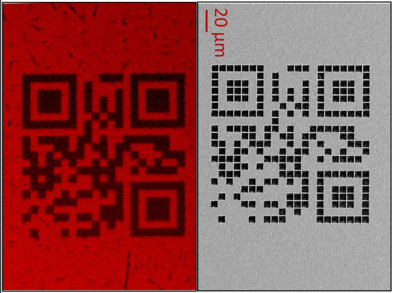
In the associated research, scientists described several applications for the new technology. The first is to inscribe information on a perovskite in such a way that it would be possible to read it only under specific conditions.
“We’ve inscribed QR codes that are invisible to anyone but the user. They can be both big and microscopic. It’s also possible to create multilayered protection: inscribe the QR code in such a way that it would be possible to read it only in fluorescent mode or when it's illuminated from a specific angle,” explains Sergey Makarov.
But that’s not all: a laser can also be used to change a perovskite’s visible color without using a colorant. The material can appear yellow, black, blue or red depending on your tasks.
“In order to give color to a surface, a laser etches special grooves that look like a lattice with a specific period,” continues Sergey Makarov. “This is called structural coloration, when a color is produced by a surface’s structure rather than a colorant. This makes it possible to produce solar cells of any color of the rainbow. In modern architecture, you can cover all of a building’s surfaces with solar cells, but few customers would like to see monotone black panels. With colored solar cells, a skyscraper can be yellow, red or blue, and yet generate power with all of its walls and its roof. Sure, the efficiency will be lower than that of black cells, but still higher than that of regular walls.”
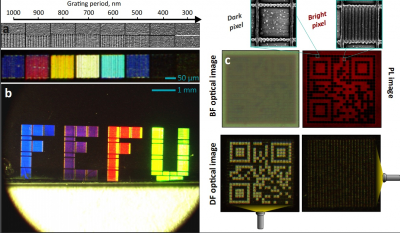
Finally, the third application is the manufacturing of nanolasers for optical sensors, and in the future - for optical computers, as well, where information will be transferred with the movement of photons rather than electrons. Finding a solution for the fast, cheap and simple manufacturing of such elements is one of the problems that stands in the way of a new age of computational technology that’s based on light.
“Light sources for nanolasers look like miniscule sticks and are usually synthesized chemically,” says Sergei Makarov. “Our research shows that they can be cut from perovskite with the help of a laser. This allows us to get thousands, tens of thousands or even hundreds of thousands of such sticks in a single minute. And all of them have the same properties, a common geometry. We hope that in the future, it will let us print such lasers right on the integrated circuits of optical chips.”
Reference: Alexey Y. Zhizhchenko, Pavel Tonkaev, Dmitry Gets, Artem Larin, Dmitry Zuev, Sergey Starikov, Eugeny V. Pustovalov, Alexander M. Zakharenko, Sergei A. Kulinich, Saulius Juodkazis, Aleksandr A. Kuchmizhak, Sergey V. Makarov. «Light‐Emitting Nanophotonic Designs Enabled by Ultrafast Laser Processing of Halide Perovskites», Small, 2020, doi.org/10.1002/smll.202000410.


