A fundamental step forward
The project in question is a continuation of a research initiative focused on Raman scattering in semiconductor nanoparticles, which has been conducted for several years by ITMO University’s Laboratory of Hybrid Nanophotonics and Optoelectronics. This effect is widely used to detect the physical states of materials and phenomena within molecules, where, depending on the chemical composition, a molecule can scatter incident light elastically or with a change in frequency.
However, the feedback signal is usually very weak: if we imagine light as a flow of photons, only one out of tens of millions might scatter inelastically and provide the observer with the necessary information. For that reason, it may take quite a while to collect the signal, further complicating the use of such measurement methods in various tasks – such as those dealing with biological processes.
The transition from spontaneous to stimulated Raman scattering makes it possible to amplify the signal by several times and, therefore, speed up the measurement process. The researchers also discovered that this method allowed them to not only measure the temperature of molecules and nanoparticles, but to efficiently increase it as well.
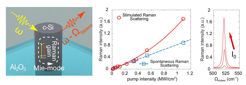
“In our earlier research, we used nanoparticles with specific geometric parameters that allowed us to enhance the Raman scattering signal owing to more efficient light confinement, which resulted in a stronger signal, but we had to wait for light accumulation within the particle. That’s why we decided to ask ourselves how we could further enhance the signal; we set a goal to optimize nanoparticles so as to facilitate a transition into a new regime – stimulated Raman scattering, which is difficult to achieve.
We succeeded in that goal through multi-stage optimization; the necessary theoretical calculations were carried out by my students – Bachelor’s student Daniil Ryabov and PhD student George Zograf, who tested them experimentally. The optimization was achieved by changing the shape and the size of the nanoparticles. We also studied the effects of a thermal sink on the process. It turned out that a nanoparticle placed on a highly-conductive surface, such as a sapphire one, makes it possible to achieve stimulated Raman scattering without overheating. The process is entirely controllable, as we can simultaneously heat up a particle and control its temperature,” says Sergey Makarov, head of the Laboratory of Hybrid Nanophotonics and Optoelectronics at ITMO University.
A non-trivial task
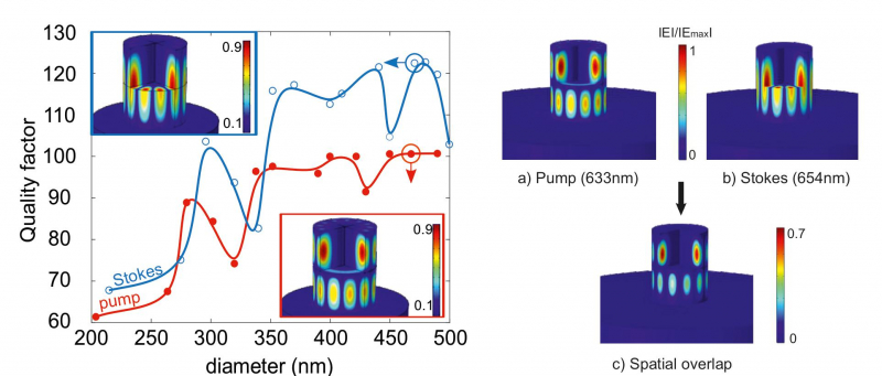
Significant contribution to the study was made by Daniil Ryabov, a third-year Bachelor’s student at the Faculty of Physics and Engineering, who figured out the most efficient parameters of the nanoparticle for stimulated Raman scattering through theoretical calculations. In order to bring about the transition from spontaneous to stimulated Raman scattering, several conditions must be satisfied simultaneously. The size of the particle and its Mie resonant properties play the key role in the process. But even if the particle is able to absorb a large part of the incident radiation, that still doesn’t necessarily lead to the transition from spontaneous to stimulated regime. It is required not only to optimize the absorption properties of the nanoparticle, but also to ensure the most efficient electromagnetic field distribution inside of it. Raman scattering operates at the wavelength of 654 nm while the particle is excited by a laser source with different wavelength – 633 nm. Therefore, the state of the electromagnetic field within the optical resonator corresponding to the Raman wavelength must somehow spatially overlap with the mode of the initial laser emission; this process is referred to as coupling and is quite a non-trivial task. Daniil managed to calculate the sizes and parameters of the entire set-up so as to meet these conditions.
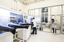
Researchers used a platform consisting of a silicon cylinder on a sapphire substrate. The disk was irradiated by a red laser beam emitted by a helium-neon laser; owing to an optical lens with hundredfold magnification, the beam was sharply focused into a spot with the diameter of less than one micron. Raman signal emerged from the sample and was collected by the same lens, which then redirected it into a highly sensitive spectrometer via a special filter.
The use of semiconductors such as silicon or gallium arsenide as resonator material provides a number of advantages. First of all, these materials significantly amplify the Raman scattering signal due to their crystalline structure properties. Secondly, semiconductor particles increase their temperature efficiently when interacting with laser radiation. The result is a ready-to-use sensing platform that acts as both a thermometer and a heating element. Moreover, implementing the platform using silicon – a key element in optics and microelectronics – will make its technological integration significantly simpler.
Next step
According to George Zograf, one of the co-authors, a PhD student at the Faculty of Physics and Engineering, and a researcher at the Laboratory of Hybrid Nanophotonics and Optoelectronics, this project has combined several findings obtained by the Faculty’s research staff: the study that concerned a nanodisk’s ability to trap light for a long amount of time (published in Science), the project that involved the world’s smallest nanolaser based on light-emitting semiconductor cubes (published in ACS Nano), and the lab’s own research on Raman scattering.
“This isn’t a final product or something ready to be put to use, but it is a highly important study from the point of view of fundamental science and a significant step forward. By combining our experience, we were able to prove the feasibility of nano-scale sources of stimulated Raman scattering. In other words, we were able to induce such a complicated concept as stimulated Raman scattering on an object that is nano-scaled in all three dimensions. If an object is very small, it can easily suffer from overheating, which is bad for any kind of optical applications. Being able to measure the temperature of a nanoparticle during the process, we managed to pump it effectively so as to induce stimulated Raman scattering but avoided overheating of the nanoobject,” explains George Zograf.
Nevertheless, the researchers already have some ideas about the project’s possible applications. Earlier on, scientists from ITMO already studied the possible use of semiconductor nanoparticles as controllable drug delivery carriers. Due to the optical properties of the particles they could be heated up effectively so that a polymer shell would easily crack when irradiated by laser and release the medicine at the right place and the right time.
With spontaneous Raman scattering, such a method would be quite difficult to apply, as the signal’s weakness means it would take a lot of time and effort to trap it. The transition to stimulated Raman scattering would make it possible to launch and control this process much more efficiently.
As the technology has a lot of potential, the researchers now plan to increase its efficiency by optimizing the parameters of both the nanoparticle and the surface:
“We’d like to continue research in this field and improve on our existing results. I assume that my Bachelor’s thesis will also focus on stimulated Raman scattering, so I’ll put all my efforts into solving this task. I think I’ll continue my studies by getting a Master’s at ITMO’s Faculty of Physics and Engineering, so it’s great to already know what my research plans are,” says Daniil Ryabov.
Reference: George Zograf, Daniil Ryabov, Viktoria Rutckaia, Pavel Voroshilov, Pavel Tonkaev, Dmitry Permyakov, Yuri Kivshar and Sergey Makarov. Stimulated Raman scattering from Mie-resonant subwavelength nanoparticles. Nano Letters, 2020.