The Faculty of Physics and Engineering: create your own nanostructure for new generation devices
The school took place on June 1-15 and involved the students of science schools in St. Petersburg. The participants studied theory and developed their own projects related to studying and modelling nanomaterials.
The work format emulates that of the “Sirius” Center for Gifted Education in Sochi. The two-week course included introductory sessions on the theory of nanotechnology and the application of nanomaterials. The participants also learned how to apply optical, probe and electron microscopes, photolithography and probe lithography. The students also learn how to edit images, present data and present the findings of their projects.
“Our goal was to optimize the way the ordered nanostructures are created. This involves a number of minor goals, but first we had to study the theory and machinery, learn how the samples are created and ultimately create them”, says Alina Efremova, one of the participants. “In addition to creating nanostructures, our tasks included conducting diagnostics on various devices: a scanning probe microscope, a scanning electron microscope and so on. Obviously, we had to come up with new ideas for the process optimization”.

Mikhail Zhukov of the Faculty of Physics and Engineering who supervises the summer school project notes that focus is on independent work as the students need to learn how to plan and conduct scientific activities.
“This year our project was creating an ordered nanostructure for new generation devices. Our students had to create a machine that would allow creating such structures quickly and inexpensively, or suggest an idea of how this can be done by improving the hardware already existing”, says Mikhail Zhukov. “In general our tasks were aimed at ensuring the independent work of participants in certain scientific fields and application of their organizational skills. It is important to take into account that the project is interdisciplinary and includes such areas as physics, mathematics, chemistry, and economics. That is why we studied both probe microscopes, that is, mechanical processing, and optical methods of diagnostics and surface modification. We also focused on theory and nanoproducts market analysis. The chemistry behind it is also important. For example, for photolithography of nanostructures and the creation of probes for probe microscope scanning one has to produce chemical reactions”.
Seven students from different science schools of St. Petersburg worked on the project. They note that they knew nothing about nanostructures before the course and yet were able to immerse themselves in scientific processes.

“We learned how to work with different equipment, create projects and present our results. It is important because we will all soon graduate and are already looking for a way to apply ourselves. I now think I want to study at ITMO University and that is why I was interested to see how science is done here, whether I chose the right faculty. We received a lot of new information here and I can say that I didn’t waste my summer, I got a great experience”, says Arina Farenbruch, a summer school participant.
Mikhail Zhukov adds that some of the experience acquired by the participants can be compared to what is usually studied in the last years of university.
“Our participants undergo serious training, they get good theoretical groundwork, experience and motivation to work further. That way they can come to university already immersed in science and start working from year one, receiving results that could be published at the international level”, he concluded.

The participants presented their work on June 15. Their project will be offered later this year on “Sirius” summer camp as a problem to solve by the students.
More than physics: measuring the speed of light with a candy bar and a microwave
Another group of pupils practicing at the Faculty was involved in computer modelling in nanophotonics. The course includes the theoretical physics studied in the 10-11th grades of school, but it is this seemingly “simple” physics that can be used to solve complicated scientific problems, notes Kseniia Baryshnikova, the course instructor and research fellow at the Faculty of Physics and Engineering at ITMO University.
Last year the participants were able to demonstrate how one can create an invisible metasurface with simple objects and also created a model of said surface. Two of last year’s participants also continued their work under the guidance of ITMO University staff. One of them, Maksim Myagkikh, has already presented at notable national conferences and is about to present internationally this fall. This year some courses on modelling and theory were repeated, but the problems offered to the students focused more on applied science.

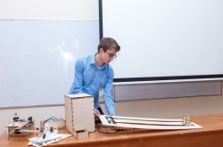
“This year we decided not to focus on metamaterials and nanostructures, but created more applied tasks without probe microscopes and high-precision lithography. We experimented with microwave, antennas and wires. For example, we investigated how to measure the speed of light using chocolate and a microwave oven. Or how to measure the frequency of a microwave oven with a wire”, says Kseniia Baryshnikova.
Students worked in groups of two and three and presented their projects on June 15. All projects are united by the general topic “Oscillations and waves”, however each of them is devoted to a separate task.
Kseniia also notes that the participants didn’t need any special knowledge. They learn both theory and practice during the summer school, and are able to conduct their own experiments and solve complex problems.
“We are developing our course knowing students will come from different backgrounds”, she elaborates. “In general, our goal is to show how we work at the Faculty of Physics and Engineering. There are many different points of view on how such summer practices should be done. Many, for example, believe that it is too early for high schoolers to do scientific work. I do not agree with that and Maksim’s example confirms that the pupils are able to engage in science at a young age. Besides, it seems very important to me to show the students how learning is different from doing scientific work and how our Faculty allows one to start really early, while still being at school”.
Biochemistry cluster summer school: synthesizing nanoink and creating smart materials
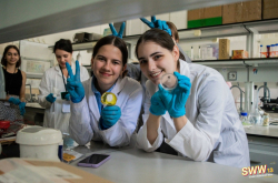
At the traditional summer school of Biochemistry cluster this year. Here the students could also immerse in scientific projects and solve problems under the supervision of a scientific advisor using the experimental and instrumental base of the cluster. The work resulted in projects that can be presented at various competitions and conferences.
As noted by Pavel Krivoshapkin, the head of the Research and Educational Center of Chemical Engineering and Biotechnology the summer school is designed for pupils of science schools who want to carry out projects in the field of chemistry and biology. The course lasted two weeks and 20 pupils of the best schools of St. Petersburg attended it this year.

Each student is given a separate task, which he or she performs under the guidance of an advisor. The tasks are diverse and include both theoretical training and laboratory work. The projects include creating a thrombolytic drug, obtaining smart materials, synthesizing nanoink for inkjet printing, getting magnetotactic bacteria and much more.
The participants of the course present their work at different conferences. Two participants already took part in the national competitions for schoolchildren: the National Internet Olympiad on Nanotechnology “Nanotechnologies - a breakthrough into the future!” and “Support of scientific and engineering creativity of high school students of St. Petersburg”, where they won prizes.
Translated by Pavel Vorobyev


