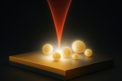
Nanolasers are smaller than the wavelength of the light they emit (or a photon). Typically, their size in all three dimensions is measured in hundreds of nanometers. These lasers are used to produce the smallest, finest parts of microelectrode devices, such as complex computers for laboratories, medical devices, and parts of game consoles. As microelectronics get progressively more sophisticated, they require even smaller components; however, because of the associated limitations, only a few production plants are capable of producing them.
Researchers at ITMO have suggested a new technology for the production of nanolasers that would meet the necessary requirements. Their invention is a cuboid-shaped perovskite nanoparticle (the lab-created material has the formula CsPbBr3). This material has been studied at the university since 2017; in this time, the researchers were able to demonstrate its stability and high optical amplification coefficient (meaning that with it, the energy of light can be used with maximal efficiency), and, most importantly, its peak performance in the green spectrum.
For a long time, this wavelength range has been so problematic for the development of compact lasers, especially industrially, that it has even been christened the “green gap.” However, with the perovskite, the researchers were finally able to crack this problem, opening opportunities for creating even smaller nanolasers: as the wavelength of green photons is three times shorter than that of infrared ones used in conventional microlasers.
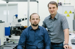
A major part of the experiments was conducted by ITMO PhD students Mikhail Masharin and Daria Khmelevskaia, while the project was headed by Sergey Makarov, a DSc in physics and mathematics and head of the Laboratory of Hybrid Nanophotonics and Optoelectronics.
“The key principle in the suggested nanolaser design is its new mechanism for building a strong light-matter connection. This helps to significantly bring down its operation threshold. As the nanolaser’s radiation is directional, it can be efficiently focused on our optical chip and registered by the spectrometer (a device for registering, processing, and analysis of light waves),” shares Dr. Makarov.
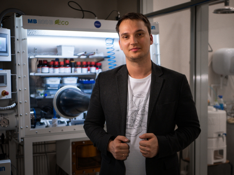
Sergey Makarov. Photo courtesy of ITMO's School of Physics and Engineering
For now, the researchers have successfully placed the perovskite nanoparticle on metal. This paves the way for a nanolaser that would be activated by electricity instead of light. Such ultracompact laser diodes, powered by electricity, could be used to create micropixels for VR headsets, medical monitors, and multifunctional optical chips.
This research project is supported by the national program Priority 2030.