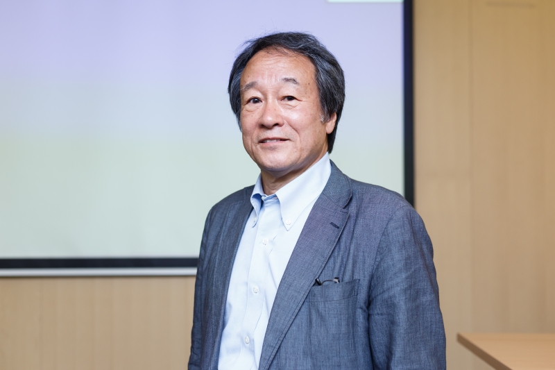
Osaka University professor Satoshi Kawata is one of the leading pioneers in a whole range of optics fields, from 3D microscopy and plasmonic nanoparticles to two-photon engineering, bio-imaging and near-field optics. The researcher has published more than 500 highly-cited papers and authored or edited over 30 books. His impressive career includes serving as President of JSAP (Japan Society of Applied Physics) and President of Spectroscopic Society of Japan. Among the scientist’s many awards is the Medal with Purple Ribbon bestowed by the Emperor of Japan.

Dr. Kawata’s work has strong links to Raman microscopy, a special method used for research and visualization of structural characteristics of nano- and micromaterials. The main advantage of this method is that it allows to keep the sample intact. Because of light affecting it on different levels, the researched object isn’t deformed in the course of the process, which enables a deeper understanding of the material’s internal structure, producing some sort of a fingerprint of the former.
Satoshi Kawata’s key research tasks include increasing the speed and accuracy of this analytical method. It is to achieve this that the scientist has been developing new devices in the field; one example is his near-field microscope with a reinforced tip. Thanks to a plasmonic particle in the tip, the device amplifies the signal and records information on the researched object with higher intensity. Pr. Kawata’s other inventions allow to decrease the surface within which the signal is collected up to five nanometers, which is a valuable contribution into the research of single nano-objects, and enable the 3D scanning with high spatial resolution.

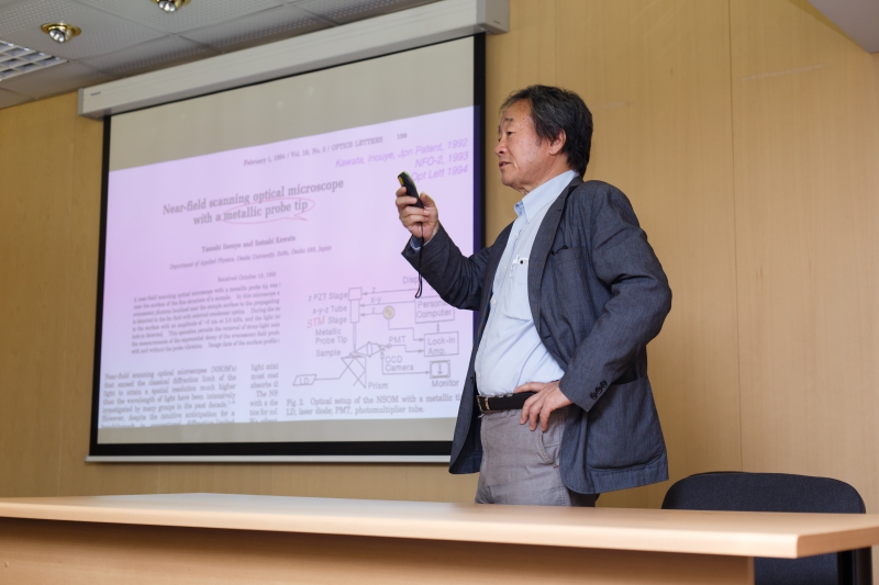
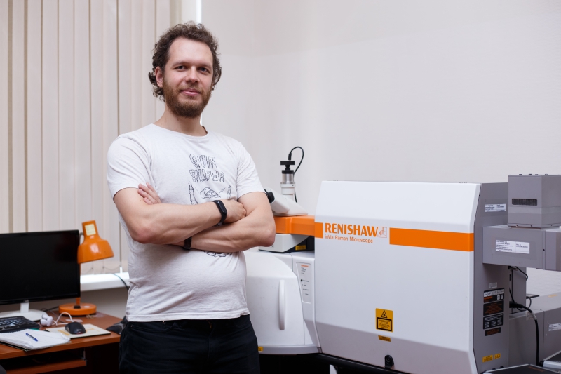
In his lecture at ITMO University, Dr. Kawata spoke about these and other inventions he was instrumental in developing. According to the scientist, he is very interested in forming acquaintances with the university’s students and staff, and also in learning more about their work. This prompted the staff of the Optical Information Technologies Center and the Anisotropic and Optical Active Nanostructures Laboratory to give the researcher a tour of their workplaces as part of which they told him about all the projects they are working on.
“Satoshi Kawata’s lecture has a direct connection to our own research, and that interested us,” says Kirill Bogdanov, a member of the Optical Information Technologies Center. “At present, our laboratory, together with Professor Rogach from the City University of Hong Kong, is conducting a joint project on light-emitting carbon dots as part of a related megagrant. Carbon dots are nanoscale objects with unique optical properties, which makes them a research priority for many of the world’s leading laboratories. The equipment available in our research center allows us to carry out in-depth studies into the structure of a large set of dots, but this technique is unsuitable to be applied to measurements of single samples. In his lecture, Pr. Kawata demonstrated the capabilities of the state-of-the-art equipment developed by his startup NanoPhoton. Using such technology makes studying single objects a reality. Such studies improve the control over the quality of synthesis and provide a more accurate understanding of the internal structure of the objects researched.”

Not only does the Japanese scientist invent different devices, but he also is actively involved in their production. Dr. Kawata is head of the company Nanophoton Corporation, which manufactures the appliances developed by the researcher. His diverse inventions can be used by science centers working in a variety of different fields, from biotechnologies to cosmetics and processing of minerals.
“Satoshi Kawata is a unique person who successfully combines research work with the practical implementation of his inventions. A lot of his near-field microscopes are now commercialized. It’s very important that he expands his broad-based academic activities with the development of devices,” shares Pavel Belov, dean of the Faculty of Physics and Engineering.


