When working on a new way of producing a specific material, researchers always have to solve a problem with several unknowns. Each new step poses new questions which must be answered. Such was the story of Russia’s first three-dimensional single-crystal gallous oxide ingot of high crystalline quality that was grown at ITMO University.
Interest towards the creation of Ga2O3 crystals first arose in the early 2010s. Japanese researchers had published a series of works on the possibility of producing such a material and its benefits of use in various electronic devices.
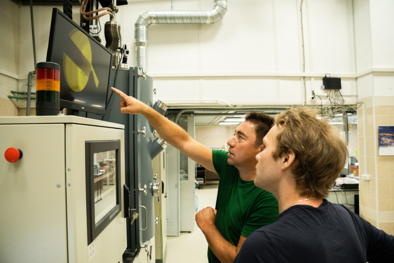
“The first Japanese articles were published in 2012-2015 and introduced the idea of gallous oxide semiconductors,” says Dmitrii Panov, a junior researcher at ITMO University’s School of Photonics and one of the authors of the study. “What made it so appealing? First of all, it is second only to diamonds in terms of the width of its band gap, which is 4.8-4.9 eV. The result is that it absorbs ultraviolet radiation, which makes it useful for, as an example, solar-blind detectors. Let’s say we are observing a rocket or missile the jet nozzle of which is emitting ultraviolet radiation – the sensor will detect that without being hindered by the Sun. Besires, gallous oxide can be used in power electronics. The results of initial research on MOS transistors, the operational voltage of which may exceed 1,000 V, are currently being published. Gallous oxide is a promising material for use in such devices. Its large band gap makes the material – and devices based on it – more resistant to ionizing radiation, which broadens prospects for its use in electronics for the nuclear industry and astrionics.”
Until recently, gallous oxide monocrystals were only produced in three countries: Japan, the USA, and Germany. But now, thanks to more than five years of work by scientists from ITMO University, they can be made in Russia, too.
Iridium crucible
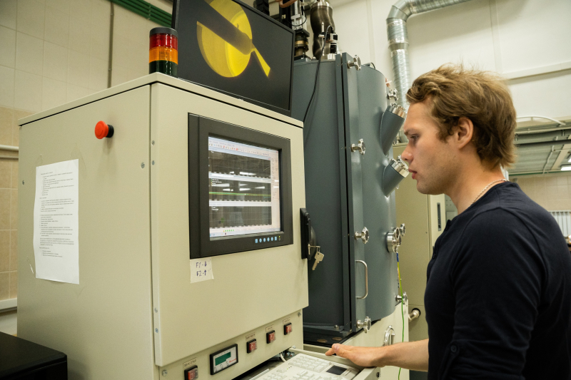
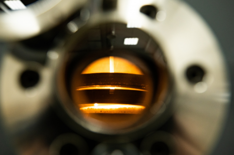
At first glance, growing a crystal may not seem like such a difficult task: Ga2O3 in powder form is poured into a crucible (a special melting vessel), brought to a temperature above the melting point, and then the melted material is used to make a crystal using the Czochralski method. A seed crystal is dipped into the crucible and gradually pulled out to produce a single-crystal ingot.
But this is where the first challenge emerges: crystals are often grown in environments filled with an inert gas (such as argon) or carbon dioxide. But in the case of gallous oxide, this wouldn’t do.
“The composition of the oxide is unstable, and it releases oxygen when melting,” explains Dmitrii Panov. “If we try to grow such crystals using argon or CO2, the molten material produces such a substance as GaO, or even metallic gallium, which forms an alloy with the material of the crucible. In the end, there’s no crystal and the crucible is corroded. That’s why the crystal must be grown in an oxygen environment.”
Oxygen, as it is known, is far from inert, which is why working with high temperatures in such an environment requires a crucible made of a special material that doesn’t react with O2. One such material is iridium, one of the most expensive metals – even more expensive than platinum. Nevertheless, even then producing a high-quality crystal requires scientists to follow a complicated multi-stage sequence of heating and cooling.
It takes one to grow one
But one of the key issues has to do with the seed crystal, which is the object dipped into the molten material to produce a crystal. The problem is that a seed crystal should ideally be a monocrystal of the substance poured into the crucible. And so, to grow a gallous oxide crystal you’d need another Ga2O3 crystal. At first, this might appear to be a vicious cycle – but it was one that researchers from ITMO managed to break.
“At first, we used a sapphire,” says Dmitrii Panov. “But the result was that different blocks would grow in the crucible, which essentially meant we produced a polycrystal.”
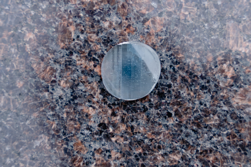
Visually, such a crystal was reminiscent of marble with lots of veins. It was absolutely unfit for use in electronics, as that calls for a solid defect-free crystal.
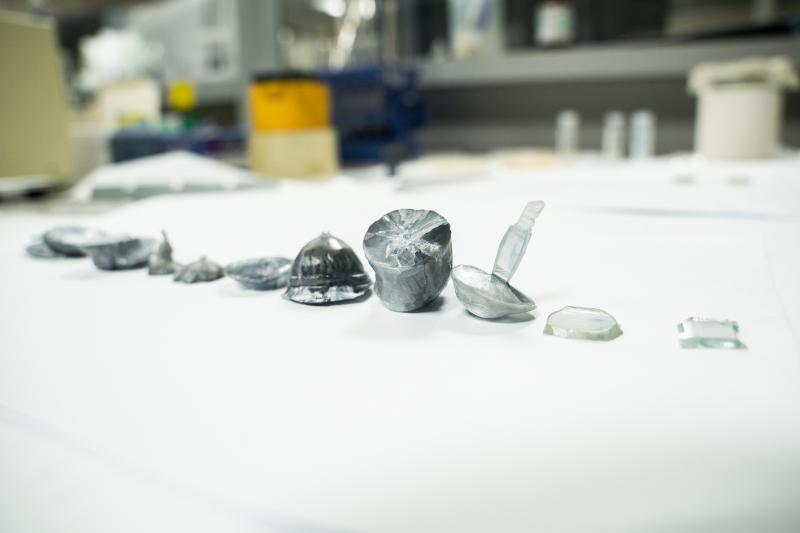
Nevertheless, the scientists were able to find among these assorted bits one that was big enough to be used as a seed crystal. It was extracted from the sample and used to grow the first monocrystal.
Future plans
Now, the researchers have to hone their technique and then they’ll be ready to start searching for commercial partners who would be capable of setting up production of much-needed gallous oxide support surfaces that would be used to create semiconductor crystals for electronics.
“Now that we’ve created a three-dimensional crystalline material suitable for supporting surfaces, we can start talking about MOS transistors and other devices based on gallous oxide. The most important task was to create the crystal itself,” says Dmitrii Panov.