What will you do at XFEL?
I will be working at the DESY science center, where XFEL's tunnel begins. Sergei Molodtsov, my science advisor from Freiberg University of Mining and Technology, works both at DESY and ITMO University; when I arrive in Germany, I'll be working in his team. The time of working with XFEL is very in-demand, yet, as it was Russia and Germany that contributed to XFEL most, research teams from these countries have priority in using it, so I believe I'll have a chance to work with the new equipment in the near future. Surely, that will be something entirely new for me, so I'll need to prepare for it; still, I'm quite sure that I'll manage, and my work in Hamburg will be most productive.
Was it hard to enter this educational program?
Well, it's not like it was anything exceptional. If one pursues a Master's program, does research, takes part in conferences and publishes papers in magazines indexed by Scopus and Web of Science, they have a good chance of entering some great joint educational program, not necessarily at Freiberg University of Mining and Technology. What's most important here is that you do science and communicate with other researchers; as for me, I've never been to any international internships or to Hamburg before.

What are the research fields the team you'll be part of works on?
The first is organic-inorganic nanocomposites; Sergei Molotsov's group wants to find nanocomposites that'll do good for resistive random access memory (RRAM). The memory elements used now are lacking, as it's volatile; as soon as we turn a computer off, the data is lost. Yet, resistive memory is non-volatile and can store information even when the computer is off. Also, the new memory will work at similar speed as modern processors, so your computer won't run slow; also, it will be able to store much data without spending much energy.
The other research field is about developing an industrial method for graphene production. This means scientists want to produce it fast, cheap and in large amounts. The new technology works like this: we take silicone carbide and apply ultra high temperatures to it, so that silicone "evaporates" from its surface. Thus, we get a layer of graphene, as a result of reshaping of the crystalline lattice of the carbon-oversaturated near-surface layer. Such graphene has a structure that can be easily reproduced from substrate to substrate and also has relatively few defects.
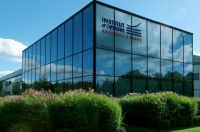
 DESY Research Center. Credit: m.desy.de
How does your former research experience correlate with what you'll be doing at DESY?
I studied at the Department of Laser Systems and Technologies, where I worked with different types of lasers: gas, solid-body, fiber and, what's most important, femtosecond laser systems; actually, my Bachelor's thesis had to do with femtosecond lasers and nanoparticles. At that time, we generated silicon nanoparticles by femtosecond laser ablation - we've irradiated silicon, it "evaporated", and we got silicon nanoparticles we then studied by different methods - scanning electron microscopy, for instance. In essence, XFEL is a femtosecond laser system as well, it's just that previously, I've been working with lasers that generate radiation in the infrared band, and this facility generates X-ray photons.
In Hamburg, you'll be also working with nanoparticles...
Yes, in the field of solid state physics - this is what Sergei Molodtsov's team is working on. I started doing solid state physics during my Master's years, my thesis topic had to do with generating silicon polymorphic modifications. Yet again, we've irradiated silicon with femtosecond laser impulses, but this time we studied the substrate and not what evaporated. Due to the high-pressure femtosecond waves, silicon with a different crystalline lattice, and hence different physical properties emerged in the substrate's surface layer. For instance, common silicon is transparent in the infrared band, but some of its polymorphic modifications are not.
Which methods used at DESY will be new to you?
Scanning and transmission electron microscopy, atomic force microscopy - all of those are techniques I've worked with at ITMO University during my Bachelor's and Master's studies, and I'll be working with them at DESY as well. Yet, X-ray photoelectron spectroscopy is new to me; it works as follows: there are synchrotron radiation sources for irradiating compounds with X-ray photons, which transfer their energy to electrons in the surface layers of a solid body and release it. An electron escapes, and special sensors are used to measure its energy. Then scientists study the difference between the energy of the X-ray photon and the released electron; this difference is the energy binding the electron to the compound. We can use all this to study how electronic structures of compounds change in dynamics. For instance, when researchers grow graphene substrates from silicone carbide, the carbide's photoelectron spectrum changes, and we can tell when carbide becomes graphene. Thanks to X-ray photoelectron spectroscopy, we can study exactly how it happens.

How is XFEL different from other existing synchrotron radiation sources?
XFEL allows us to develop a diffraction pattern of laser impulses' interaction with the compound, which can be used for recreating the compound's structure. The facility generates ultrashort pulses with a very high photon density; the amount of photons in just one impulse is enough for developing the whole diffraction pattern. This allows for studying biological molecules without crystallizing them, i.e. in their natural state. Under the effect of laser radiation, molecules disintegrate quickly, yet XFEL's impulses are so fast that they can collect all the information necessary before that happens, as their burst time is faster than the speed of a chemical reaction (you can read more about how XFEL works here).
Did you know about XFEL before?
Not before I got interested in a joint program with Freiberg University of Mining and Technology. When I started to learn more about this new facility, I was startled at the opportunities it offers, as it allows to record a chemical reaction frame-by-frame - i.e. really see how a compound's molecular structure changes. Earlier, scientists didn't have access to such opportunities. Some, I think, have been waiting for years to get them, and many will rush to conduct experiments. This is why I believe we can expect many new advances in the near future.

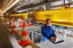
XFEL facility. Credit: twitter.com
Do you think people who are not scientists must know what XFEL is for?
I think it's important for younger people who have to decide on their future. Many believe that being a scientist is not a proper occupation, but something strange. It would be great if young people understood that they can well become scientists, that it is a serious and interesting job. This is why we need to show that everyone has these opportunities; when I only entered the university, I never imagined that I'll get to work at such a world-renowned facility. What's most important is to study, train, and then you'll get an opportunity to partake in something superb.
You never thought you would become a scientist when you entered ITMO University?
Before entering the university, I've studied at ITMO's Laser Technologies School for school students; we got lectures about lasers and conducted simple projects. When you've already spent much time working in laser laboratories, it's nothing much, but when you're a kid and see it all for the first time, it really inspires you. Truth be told, I didn't exactly know what I'll be doing once I graduate; it was just that I was good at physics, and didn't know what to do with it. At the Laser Technologies School, they've explained to us that lasers are a promising field, and they have many applications. And I never regretted studying at the Department of Laser Systems and Technologies; when I was already a Master's student, I became head of this Laser Technologies School and worked with school children in the laboratory. By the way, the admission is now open, so, school children - welcome!