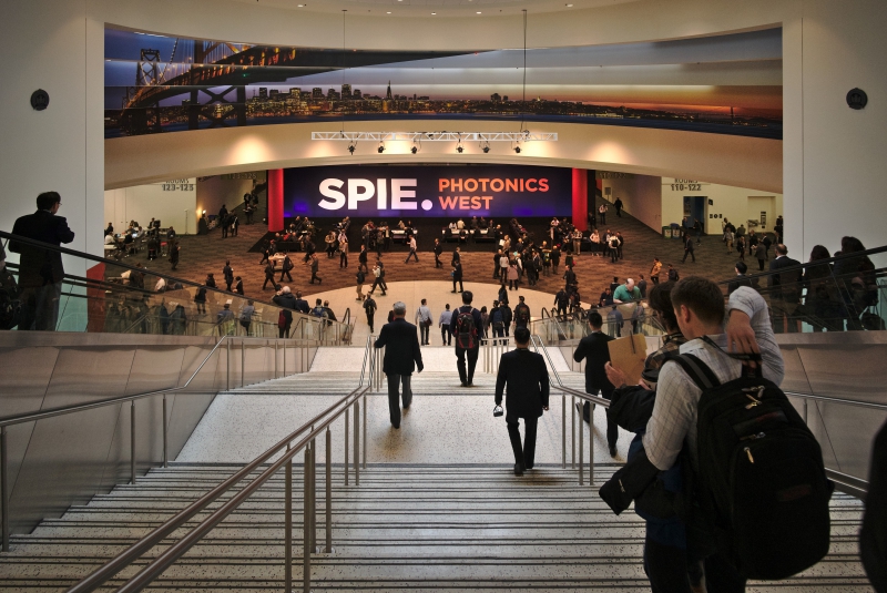
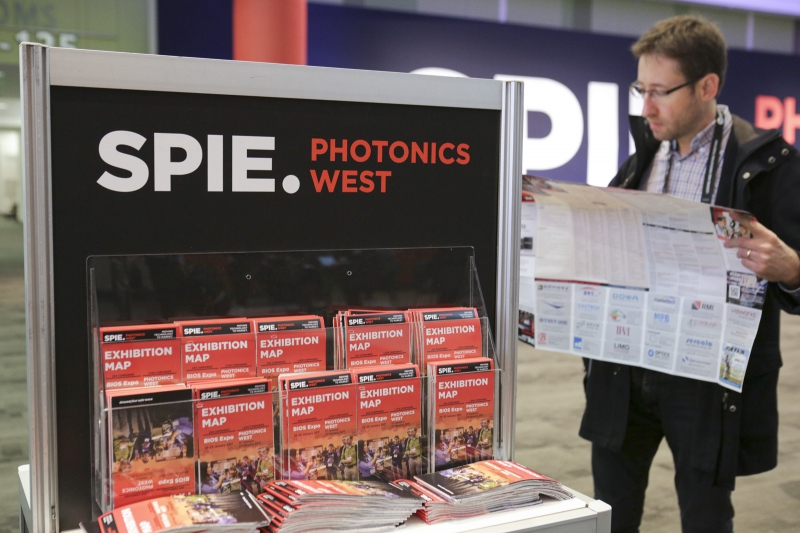
SPIE (Society of Photo-Optical Instrumentation Engineers) is an international nonprofit professional society of scientists, engineers and students interested in optics and photonics. SPIE brings together over 17,000 members from all over the globe, including members of some 100 student organizations. The society runs ten scientific journals and a digital archive with over 235,000 online articles, and organizes more than 140 workshops and conferences all over the world annually. Supporting aspiring scientists is among the key areas of focus for the society. Students and researchers from any country can apply for the scholarship, which covers tuition fee, learning materials, research expenses, as well as other expenses associated with education.
This year, five ITMO University researchers have been awarded the SPIE scholarship. Just as last year, the university topped the list in terms of the number of winners. In total, 75 scholarships were awarded to scientists from the US, Canada, Germany, the UK, Finland, Estonia, Argentina, Romania, India, Ireland, Australia, Columbia, Ukraine, Belarus, Poland, and Russia.
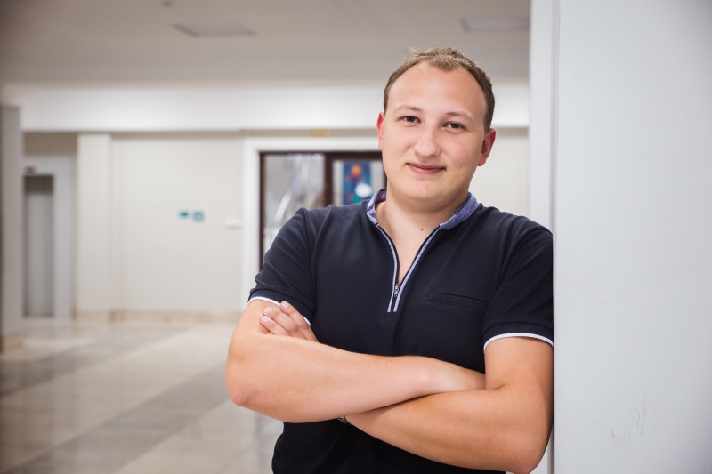
Tatiana Vovk, engineer at the Faculty of Photonics and Optical Information, member of Laboratory “Modeling and Design of Nanostructures”
Modern technologies such as smartphones, lasers, microwaves, and the internet have become part and parcel of our daily life. However, all these things would be impossible without physical discoveries of the 20th and 21st centuries, which, in turn, owe their existence to quantum field theory.
What makes quantum physics different from classical physics is that in classical physics, you can know everything there is about a system and predict the future with certainty, but the future in the quantum world is less certain. In quantum physics, experiments are conducted to work out new exotic laws. These are the laws that the microscopic world around us – the world of atoms, molecules and elementary particles – abides by. It took people quite a long to time to start taking this “new physics” seriously, but over time, a great number of exact matches of the quantum theory with experimental results made the humanity understand its importance and relevance.
Though it is quantum physics that accelerated the latest technological breakthrough, no one fully understands how it works. What scientists do is they simply use its laws for forecasting physical effects. No one can be completely sure if these phenomena are real or not, because you cannot see them occurring with your own eyes. That’s why it’s crucially important to transport the laws of quantum physics from microworld that we cannot see to the systems of macroworld. To achieve this goal, a lot of tricky experiments are conducted in the world’s leading laboratories.
My work is dedicated to one of such experiments. I do theoretical research into deep laser freezing of dielectric nanocrystals doped with ytterbium ions in the field of a radiofrequency trap. Ytterbium ions make nanocrystals to absorb photons from the laser. As a reaction to each absorption act, a recoil impulse is communicated to the nanocrystal, slowing down its movement. A dielectric nanocrystal with ytterbium ions has an uncompensated surface-bound charge, which makes it possible to suspend it in the electric field of a radiofrequency trap.
In my research, I propose to cool the nanocrystal to temperatures close to zero, which coincides with its transition to a macroscopic quantum state. In this state, the nanocrystal starts to develop quantum properties. At the same time, it is too big to be an object of the microworld and too small for people to be able to see it with the naked eye. Such ultracold quantum nanocrystals are thus the first step towards people understanding the laws of quantum physics.
As for my plans for the future, I want to research the phenomenon of energy exchange of nanocrystals’ movement and their crystalline lattice.
SPIE scholarship
In my opinion, what really helped me to get this scholarship was a good application. To win the scholarship, don’t just say that you need money, but describe how you’re going to use this money. If you read the competition’s rules carefully, you’ll see that you can spend the money on learning materials in the field of optics and photonics, as well as online courses and internships related to physics, programming and photonics.
Apart from that, you’re also expected to demonstrate your scientific and/or teaching potential, that is to share with the competition committee about your current work and future plans, and also about what inspired you to study photonics and optics. Make sure to mention all your previous awards and submit a good resume.
I will use my SPIE scholarship, first of all, to cover the expenses on my internship at the Laboratory of Photonics and Quantum Measurements at the École Polytechnique Fédérale de Lausanne, where I plan to purchase some learning materials and take several online courses that I need for my future work.
Valery Kozin, engineer at the Faculty of Physics and Engineering, member of the International Laboratory of Light-Matter Coupling in Nanostructures
Right now, I’m doing research on strongly correlated multi-particle systems, namely in the context of the quantum time crystal task and quantum transport phenomena in disordered media. Also on my current agenda are polaritonics tasks, phase transformations and relevant research done using machine learning methods. I received my SPIE scholarship for my work on optically-controlled mesoscopic devices, polariton topological insulator and proposed method of identification of phase transformations in magnetic systems with the use of machine learning methods.
The results of my research can be applied in promising spintronic/spinoptronic devices. There is a range of tasks that mostly belong to the realm of theoretical physics, for example, the task on quantum time crystals. For a long time, it was believed that systems like these just don’t exist in proper, there was even a theorem that was proven on this topic, but we are currently working on finishing touches to the work that posits this proposition. The system we are considering can hardly be implemented in practice, but it nevertheless answers the question set forth in 2012 by a Nobel Prize in Physics laureate Frank Wilczek about spontaneous breaking of translational symmetry in time.
SPIE scholarship
This has been the third time that I applied for the scholarship, and the judges seem to have appreciated the work I’ve done during the last year and a half of my PhD studies, when I started to actively publish articles on the topic very close to that of SPIE. Before that, in my Master’s studies, I used to research the Yang–Mills supersymmetry theory, which falls out of the Society’s focus.
The lion’s share of my research is conducted on computer, as modern theoretical physics often goes hand in hand with the computational one. That’s why I plan to spend some of my scholarship money on improving the productivity of my PC. Another part will go on books. In the future, I plan to continue my research on highly-correlated many-particle systems, and also to try my hand at quantum informatics tasks.
Anna Vasilyeva, junior research associate at ITMO University’s Research Center for Optoelectronic Instrumentation Engineering
My research focuses on the visualization of ionizing radiation. Together with my colleagues, students and PhD researchers at the Faculty of Applied Optics, I work on developing a system for visualizing gamma radiation. We got the funding for this project by winning a competition of practice-oriented research, development and technological works held by ITMO University. Our project is now nearing its conclusion, but we plan on continuing our research in the future. The results of this work will be included in my thesis.
One of the most important applications for this research is in safety systems on radiation hazardous sites. Visualization of ionizing radiation will allow to conduct radiation monitoring that is highly discerning and effective. Development of radiation monitoring devices has always been a topical and important task. I think that now, what with the airing of the HBO TV series Chernobyl, more and more people in the wider public will become interested in these systems.
The end goal of our project is, of course, to launch our visualization system on the market and see it implemented on radiation hazardous sites and places of mass gathering of people. We need to carry out a multitude of theoretical and experimental research to get there, from ways to bump up the quality of final images to expanding the range of energies registered and improving performance parameters. These are the main objectives for our future research. I believe that what we do has a lot of potential both in terms of theory and practical applications.
SPIE scholarship
It is indeed very hard to get a SPIE scholarship as the number of candidates increases year in year out. To ensure your success, it’s important that your application mentions something about your motivation, your desire to contribute to modern science, and willingness to share your knowledge with others. You have to be really inspired by everything you do to pull that off. Another aspect worth focusing on is showing your professional growth and development, starting from the very beginning of your university studies. I paid a lot of attention to all of that when preparing my application.
Any achievement, especially of such a high level like the SPIE scholarship, is first and foremost a boost to one’s motivation. Having your work recognized gives you a stimulus to develop, accomplish new results and share them with the scientific community. My plans for the near future include presenting my research at the SPIE Optical Metrology conference.
Oleg Ermakov, engineer at the Faculty of Physics and Engineering, member of the International Research Center for Nanophotonics and Metamaterials
If you throw a stone in water, you’ll notice waves rippling on the water surface. The topic of my research, electromagnetic surface waves on two-dimensional structures, is analogical to that. These waves create a strong localization effect on electromagnetic field close to the structure, depend on the direction of their propagation and have interesting polarization properties. Looking ahead, these waves can become manageable carriers of optical signal and find application in optical data processing systems. They are already used for tasks of detecting various biological objects.
Another direction of my research is discovering polarization degree of freedom of localized waves. In free spaces, polarization-based degeneration of electromagnetic waves spectrum just happens by itself. This is the basic operating principle for all polarization devices, and flexible management of polarization is widely used in microscopy, cryptography, ellipsometry, sensors and other fields of optics. But there is no polarization degree of freedom for localized surfaces and waveguide modes.
My aim is to research the relevant physical principles and create structures that would support localized electromagnetic waves with a polarization-based degenerate spectrum. This will allow to create analogues of classical polarization devices for waveguides and planar technologies, and to improve many existing optical technologies. This research is supported by grants from Russian Foundation for Basic Research, Russian Science Foundation and the Foundation for the Advancement of Theoretical Physics and Mathematics “BASIS”.
The project’s future development is in experimental validation and implementation of theoretical results obtained. This work has already started and is now being actively developed as part of a research collaboration with leading research groups under the guidance of Andrei Lavrinenko from Technical University of Denmark and Yuri Kivshar from Australian National University.
SPIE scholarship
First and foremost, receiving a SPIE scholarship make you confident that you are pursuing topical and important research that is valued by the international scientific community. Thanks to the scholarship, I am now planning to attend the SPIE Optics+Photonics 2020 conference that will be held in San Diego, the US.
What makes or breaks your success in getting the scholarship? It’s a difficult question I have thought long and hard about but still failed to find a definitive answer. Of course, the main criterion of success is the topicality and significance of the research conducted, as well as a candidate’s personal achievements.
Apart from that, what possibly helped me win are my efforts on popularizing optics and photonics among the wider public (I often hold science-pop lectures on physics for school and university students and open lectures on photonics and physics, namely this one) and good competition record. Two years ago, I had won a SPIE Travel Scholarship, which I used to travel to the SPIE Optics+Optoelectronics in Prague and won the Best Student Paper Award there.
Ekaterina Tiguntseva, engineer at the Faculty of Physics and Engineering, member of the Laboratory of Hybrid Nanophotonics and Optoelectronics
My work mostly revolves around research of optical properties of nano-sized light sources based on organic-inorganic perovskites.
My acquaintance with this class of materials stems from a review that contained the latest advances in the field of perovskite-based nanophotonics. In two years, I have studied the optical properties of thin perovskite films and different nanoparticles, resonance perovskite nanoparticles with reconfigurable light-emitting properties, and waveguide properties of periodic perovskite-based nanostructures. Substantial interest to works on these topics attests to the fact that my research field really is very relevant.
At the moment, I’m continuing my work in the field of hybrid nanophotonics, with my main research topic being nano- and micro-lasers based on perovskites.
Research of the fundamental properties of these structures and creation of highly effective nano-sized light sources will potentially allow for them to be applied in optical chips, LEDs and solar elements.
SPIE scholarship
What allowed me to become a winner of the SPIE Optics and Photonics Education Scholarship 2019 was the significant volume of work I had conducted in my research field and a strong CV that arose from the latter.
Obtaining an international scholarship of this level really bolsters your motivation to work and do your best. It also provided me with funding to carry out an experimental research trip to obtain new experience and contribute to the development of international cooperation in my field, and to update my equipment which also plays a huge role in research work.