ITMO Researchers Suggest New Laser Microscopy Method
At the foundation of the new method is the phenomenon of Raman scattering. If the researchers’ idea is implemented practically, its use will help expand the possibilities of laser microscopy. An article on the subject was published by Advanced Photonics Research.
The objects of researchers’ studies are becoming increasingly smaller. Scientists desire to know how chemical bonds in proteins can unfold due to thermal effects, or how cell organelles react to light. Therefore, a number of optical non-invasive tools are being suggested as means to visualize experimental studies at the submicron scale.
This is why scientists are constantly looking for ways to improve, reduce the cost of, or simplify the methods of optical microscopy and spectroscopy. Some of the solutions lay with laser microscopy and spectroscopy, wherein the images are produced in the following manner: an object, such as a protein molecule, is subjected to intense electromagnetic radiation near an optically resonant nanostructure, while a device registers the molecule’s reaction towards the radiation by re-emitting the light at a shifted frequency.
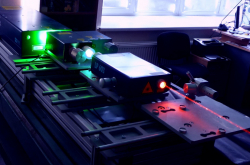
“In such cases, a powerful laser is focused on nanostructures made of metal or semiconductor particles,” explains George Zograf, a junior research fellow at ITMO University’s Faculty of Physics and Engineering. “The electromagnetic (EM) field between two nanoparticles is localized and can therefore amplify the emission produced by the nanoobject – either a protein molecule or an active material with a unique optical spectrum. There are a number of spectroscopy and microscopy methods that use metal probes. Such probing was implemented by our colleagues back in 2015 for silicon dimer nanoantennae. With their approach, the probe detects the near EM field while situated several dozen nanometers from the nanostructure. But this near-field method is quite sensitive to mechanical vibrations and is rather time-consuming, making it ill-suited for some practical applications.”
Triangle structure
Scientists from ITMO University have suggested a new way to improve the method of optical microscopy and visualization of localized EM fields with the help of Raman scattering. The researchers took three silicon nanodisks and placed them at an angle towards each other so as to form a triangle towards each other. Such a placement results in a noticeable amplification of the EM field. For that reason, the laser source no longer needs to be as powerful and there is no risk of heating up the surroundings of the nanostructure. Moreover, it is no longer necessary to keep the source close to the silicon particles. Better yet, this change should not reflect on the accuracy of studies.
“Our approach makes it possible to quickly and remotely study the optical response of a system using Raman scattering and with the help of only a laser and precise positioning,” explains George Zograf. “As a result, the scattered light may either acquire energy from these oscillations or lose an amount of energy equal to the energy of the oscillations. The spectral features of scattered light differ from the spectrum of a laser. We can use the spectral features and the change in the intensity of Raman scattering to determine the resonance qualities of nanostructure or the chemical composition of compounds, as each material has its own unique optical Raman footprint.”
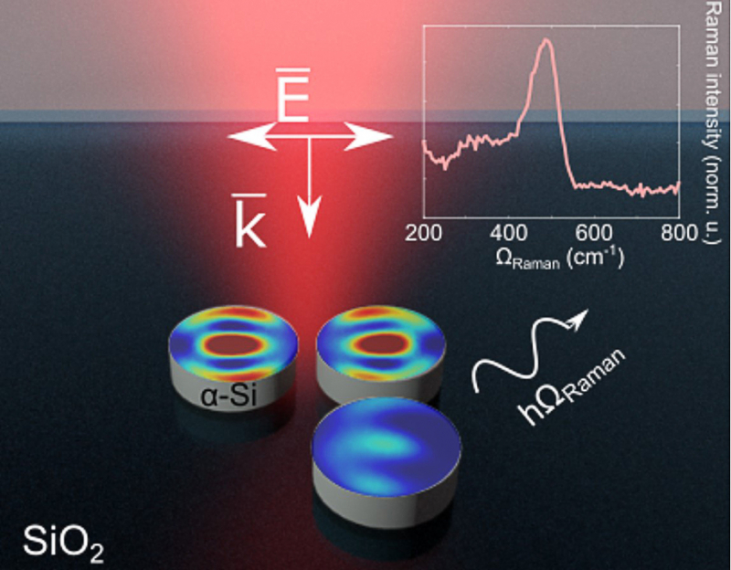
The proposed geometry of the nanostructure has another advantage. By changing the polarization of light and nothing but, scientists can use light to sequentially excite just one or another pair of nanodisks. This allows them to selectively study processes that occur in different points of a sample with high spatial resolution. This, as well, opens up new opportunities for complex study of chemical and physical processes at the nanoscale.
“In my experiments, I used a high magnification lens and a platform for precise sub-100 nm positioning of samples to acquire a map of the EM near-field surrounding the nanostructure. Surprisingly, the resulting Raman scattering intensity map matched with our theoretical calculations even better than the conventional near-field optical microscopy method. I carried out multiple measurement rounds with various nanostructures and polarizations so as to be completely confident that our new method is quite effective and versatile,” adds George Zograf.
Collaboration

The research paper was published in the new scientific journal Advanced Photonics Research, which is put out by the well-known international publishing house John Wiley & Sons. The journal’s editorial board extended a special invitation to the scientists from ITMO, asking them to join one of the journal’s first issues.
“Being invited to join the first issue of such a promising journal is a sign that the research done by scientists at ITMO University sets the tone for scientific work around the globe. Every new journal wants to gain a flawless reputation by publishing high-quality articles by the best research centers. The journal’s editorial team includes renowned scientists from countries that lead the way in physics research; every article is carefully picked. Despite us being invited to publish the article, we still had to pass several rounds of reviews by experts in the field – which, no doubt, only served to improve its quality,” explains Sergey Makarov, a senior research fellow at the Faculty of Physics and Engineering.

Sergey Makarov, a researcher at ITMO University and a co-author of the paper, has been invited to be a part of the journal’s advisory board for a period of three years. His responsibilities will include reviewing articles, selecting authors to be invited for publication, helping choose the subjects of special issues, and expanding the geographical scope of the journal’s author and reader audience. The key task of the journal’s advisory board and its editorial team is to earn it a place among the most renowned and leading journals in the field of photonics.
Reference: George Zograf, Kseniia Baryshnikova, Mihail Petrov, Sergey Makarov. Enhanced Raman Scattering for Probing Near‐Field Distribution in All‐Dielectric Nanostructures. Advanced Photonics Research, 2021/10.1002/adpr.202000139