From lasers to nanophotonics: finding a calling
My path in science began long before ITMO. First, I studied physics at Volgograd State University; then, in 2009, I started my PhD at the Institute on Laser and Information Technologies of the Russian Academy of Sciences. I was driven to pursue science in the conventional sense: I wanted to have academic freedom, come up with innovative solutions, and always learn something new – that’s why it only made sense for me to get my PhD.
At the university, I investigated how laser radiation interacts with matter and how this can be used to shape and change the properties of materials for microelectronics. I defended my thesis in quantum electronics and earned my PhD in 2012.
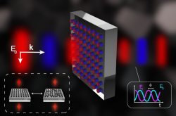
After my defense, I had to make a choice: to keep pursuing my field or try something new. I chose the latter: in 2015, I joined ITMO’s Metamaterials Laboratory, and for the first time, I began to seriously get into nanophotonics, namely, the fundamental end of the field: resonant metal-dielectric nanostructures. These are artificial nanobjects made of a metal and a semiconductor. While metals are good at amplifying light, they suffer from high heat losses; semiconductors, on the other hand, generate almost no thermal energy but fail to strengthen electromagnetic fields. Together, they trap light at the nanoscale, amplify it, and transmit it in a desired direction – all this is necessary for creating compact optical devices and sensors.
We began combining metals and semiconductors into single nanostructures; that’s what hybrid nanophotonics does. Over time, a team formed around these efforts, and with it – new tasks and projects.

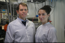
The team of Interdisciplinary Technologies Center (ITC) “Bridge.” Credit: Dmitry Grigoryev / ITMO NEWS
From an idea to a team: the grant that changed everything
The team didn’t grow instantly; it happened gradually. First, I had some ideas that I could pull off on my own, but as the work piled up, students started joining me. Once they had defended their theses, they had to decide where to go next. The problem is, though, it is not always easy to secure funding for your research; for some, it takes six months, while for others – a year. To fix this problem and keep key specialists on the team, we applied for the grant under the Team PI track – this is a standalone opportunity created at ITMO as part of the Priority 2030 national program. We got it in 2023 and were able to build a system where people can come, grow, and stay in science. Before that, we had about 10 people on the team, but then we started growing fast – both in tasks and people.
The grant support focused on training future specialists by engaging students in research as early as high school or the first years of their Bachelor’s studies.
To start this process as soon as possible, we opted for ecological nanofabrication, which involved the creation of functional nanostructures without using toxic reagents or complex processes. Put simply, this approach is designed to make nanoobjects, like silicon nanoparticles or metal nanoantennas, easier to produce. We didn’t make them in expensive cleanrooms with multi-step processes; instead, we used laser processing and other simple methods that are quick to pick up. This way, newcomers could build a working prototype on their own, see their ideas come to life in just several weeks, and get actively involved in research.
A school student becomes a first author
The grant not only provided funding, but also helped us structure our work. We used to focus on several fields related to nanophotonics, but once we received the funding, we started to work with school students, interact with industries, and do progress reviews. All these diverse tasks quickly forced me out of my comfort zone. It’s one thing to lead research, but it’s a completely different story to manage a project where everything revolves around helping people to grow.
I had my first report sessions; there, you have to quickly sum up what you’ve achieved and where you fell short, and whether you managed to adapt to external factors. This experience helps me a lot when I need to pitch my ideas to investors and experts – and that’s vital for finding partners for applied projects and launching your developments into the market. And this wasn’t just about me; the team, too, grew in these three years. We published a series of papers in Nature Index and the top 3% of SJR, including Light: Science & Applications, Advanced Materials, and Laser & Photonics Reviews.
For example, Martin Sandomirskii, a Master’s student at ITMO’s Faculty of Physics, was a school student when he first joined us; by the end of his Bachelor’s studies, he was already a first corresponding author of a paper in Nature Communications that had ITMO staff as 80% of the contributing researchers.
A bridge between fields: how physics and biology meet
Once the support within the Team PI grant came to an end, we chose not to stop at what we’ve achieved and continued to lean towards nanophotonics and applied optical systems (nanostructures that interact with light). Meanwhile, also at the faculty, the team of associate professor Mikhail Zyuzin was working on functional nanomaterials for biology and medicine; they specialized in drug delivery, photothermal therapy, cells, and animal models.
Our tracks complement one another perfectly: we know how to produce light-responsive nanostructures, and biologists from Mikhail’s group know how to deliver them to the target area in the body and work with cells and tissues. By merging our teams, we were able to complete the end-to-end cycle of nanostructure development – from synthesis to application in biological systems. This very intersection gave rise to the Interdisciplinary Technologies Center (ITC) “Bridge,” which serves as a bridge between fields, subjects, and people.
Inside the center: spaces and tasks
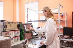
Currently, the center is home to two key teams. They run joint projects but also maintain their distinct research areas, tasks, and expertise. In total, we have around 40 people: Bachelor’s, Master’s, and PhD students, as well as postdocs. They all work in a shared space with shared equipment: laser systems, spectrometers (devices for measuring the light spectrum), microscopes, as well as chemical, optical, and cell laboratories. Because of this, we can quickly find a team for any task; if a project needs expertise in both optics and biology, both teams step in.

Preparation for chemical synthesis. Credit: Dmitry Grigoryev / ITMO NEWS

Inside a cell laboratory. Credit: Dmitry Grigoryev / ITMO NEWS

Experiments on the assembly of hybrid nanoparticles. Credit: Dmitry Grigoryev / ITMO NEWS
Current projects: biosensors, unclonable tags, and industrial projects
At the center, we continue to develop subjects we got into several years ago and also introduce new ones. One of the main focuses for us right now is biosensors – nanophotonic structures that can detect disease markers via changes in optical responses. Nanostructured surfaces are modified to bind with specific molecules – such as protein markers or the fragments of DNA pathogens. Once a molecule sticks to the surface, the refractive index of the surroundings changes – and so does the color of the nanostructure. This change can tell us which marker is present in the sample and at what concentration. This can be used to produce express tests that will outperform traditional lab tests in terms of speed and cost.
Another project we’re currently working on is about physical unclonable security labels made from silicon nanoparticles. They can’t be counterfeited, as their structures are formed randomly. We take a silicon film and use a laser to blast nanoparticles out of it – they scatter across the surface in a random pattern, like grains of sand spilled from a glass. Each resulting pattern turns out unique and can’t be reproduced even by the person who made it initially. The pattern is then digitized via a microscope and uploaded to a cloud database; to verify authenticity, you need to upload a photo of the tag into the system. These labels can be applied to products, documents, and packages – anything that needs anti-counterfeit protection.
Martin Sandomirskii and Pavel Kustov brought this technology to an MVP and presented it at the international exhibition GITEX Global in Dubai in 2023. Today, we continue to advance this project to find its industrial application.

Working with silicon nanoparticles. Credit: Dmitry Grigoryev / ITMO NEWS
Another field is microfluidics – namely, systems for controlling small volumes of liquids needed for laboratory analysis and diagnostics. We also use AI in photonics; we create algorithms to process experimental data, predict the properties of nanostructures, and automate the analysis of optical spectra.
Separate teams work on their own projects, too. For instance, the team of Vitaly Yaroshenko develops resonant nanostructures with embedded ions of rare-earth metals – elements that interact with light in the telecommunication band where signals are transferred via optical fibers. These structures can help produce devices for processing optical signals.
The merge came with new fields, as well. One of them is nanomedicine – the field in which nanomaterials are loaded into therapeutic agents to reach the target site in the body. The materials for nanoparticle carriers, as well as delivered agents, can vary depending on the task. At the center, we can conduct both synthesis and complex biological experiments.
“The industry set tasks that go beyond labs”
In addition to research, the center also conducts applied projects for the industry. One of our partners is NTO – a major Russian producer of specialized technological equipment for electronic and semiconductor production. Together, we’re developing an in-situ control system and plan to take this technology to serial production.
This collaboration is especially valuable to us since the industry sets tasks that are hard to simulate in laboratories. We also design tools, reverse engineer existing solutions, and develop microfluid and sensor systems – everything that is somehow related to optics.

Microfluid synthesis. Credit: Dmitry Grigoryev / ITMO NEWS
Student ideas become startups
Our center isn’t only about projects; we also help those who want to turn their ideas into products. Several people at the center received grants from the projects UMNIK and Student Startup – thanks to them, they can develop their lab samples into an MVP and present it to potential buyers. For example, Master’s students Van Gulinyan and Daria Sennikova, alongside PhD student Pavel Filatov, are working on sensor systems, while junior researcher Konstantin Arabuli is working on a student startup project. Turning our results into actual products has been a completely new experience for us. We also attend venture forums where startups look for investors and partners.
Additionally, we make use of other support tools for young researchers offered by ITMO and other organizations. For instance, Rising Star is a contest and school for scientists who have just defended their theses or are about to complete the final year of their PhD program. There, they can improve their management skills, build a team, launch their own research track, and even become a research lead. This is an excellent chance for young specialists to stay at their alma mater after graduation and for ITMO – to not lose valuable specialists.
Interdisciplinary Master’s: training hybrid specialists
A major milestone for our center became the Hybrid Materials track in the Master’s program Advanced Quantum and Nanophotonic Systems.
Just like the center, the track is interdisciplinary; thus, it welcomes students from various backgrounds – physicists, chemists, biologists, and experts in materials science. All are trained by developing applied projects with their mentors. Students study numerical modeling (the ability to predict how materials and structures will behave), as well as materials science, nanophotonics, organic chemistry, and cell biology. They work on specific tasks: metal-organic frameworks, porous materials for drug delivery and purification, targeted drug delivery, and biosensors that detect biological molecules. Our specialists have expertise at the intersection of different fields and start their own research tracks at the center.

Optical scheme assembly. Credit: Dmitry Grigoryev / ITMO NEWSOptical scheme assembly. Credit: Dmitry Grigoryev / ITMO NEWS

Setting up the photoluminescence lifetime measurement system. Credit: Dmitry Grigoryev / ITMO NEWS
Plans: fundamental science to market
We intend to continue our fundamental research in nanophotonics – it’s vital for our future applied projects. At the same time, we’re going to develop biosensors and create prototypes we can later pitch. We’d also like to strengthen our collaborations, attract new partners, and bring our products into the market through startups, grants, and joint industrial projects.
As a result, everything we do – science, partnerships, and products – is made for people.
Many of our students opt to stay at the university: they defend their theses, become researchers, and build their own teams. Some break into the industry but keep in touch with us. Teamwork experience is an advantage in any job interview. That’s why our center provides the exact foundation a person needs to grow and find their place in the professional world.
How to join the center
Our center welcomes students of all levels. We don’t have any strict limitations on the number of researchers; if a person is motivated, is driven by science, and has the required competencies, we’d be glad to have them on our team.
To join the center, you need to study our website and select a field of study you’d like to pursue. Then, you can write to me, Dmitry Zuev (dazuev@itmo.ru), Mikhail Zyuzin (mvziuzin@itmo.ru), or any other specialist at the center, and tell us about yourself and list the tracks you’re interested in. In some cases, we can tell if a person is a good fit for us at this very stage. If successful, you’ll be invited for an interview where we will evaluate your experience, as well as your thoughts, interests, and readiness to study.
Newcomers start off as assistants: they are mentored by more experienced experts, learn, and try to take on more complex tasks. After some time, they can start their own independent research or manage a module or a small group. This happens differently for everyone – some are ready by the end of their Master’s, while others need more time. The main thing is that we provide an environment where you can grow.