The Advanced Materials Week conference takes place at ITMO University’s campus on Lomonosova Street, 9. Scientists from France, Canada, Sweden, Finland, Japan, and Russia have gathered in the assembly hall to discuss new materials required by the accelerating technological progress.
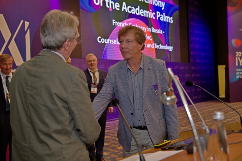
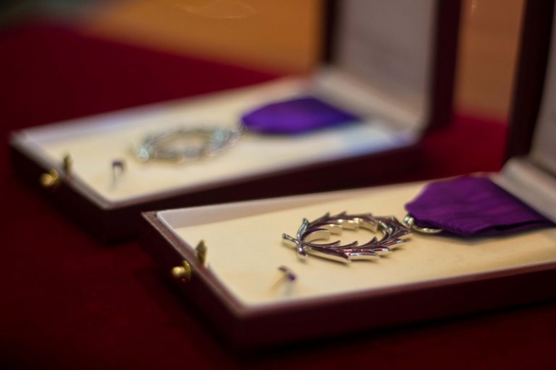
Among the organizers of the event’s first section is Vladimir Dubrovskii, recently named a Knight of the Order of Academic Palms (Ordre des Palmes académiques). This award, established in 1808 by Emperor Napoleon Bonapartes, remains France’s highest decoration for those who have contributed to the development of science and education. We’ve managed to speak with Prof. Dubrovskii during a break between the sections of the conference.
First, allow me to congratulate you on your award. What does it mean to you?
Thank you! I am now a chevalier, or knight, of the Order of Academic Palms. There are three grades of it, up to the title of Commander. Any award, of course, is always a pleasure. For me, this is first and foremost a recognition made not just by me, but my team and my lab, which I’ve headed for many years, into the development of nanophotonics.
We’ve long collaborated with various French research teams. Our main partner in France is the Center for Nanoscience and Nanotechnology, now a part of the Paris-Saclay University cluster. One of my colleagues and friends is professor Frank Glas, an honorary member of the Ioffe Institute. For the past ten years, we’ve headed a joint Russian-French laboratory that unites a number of research teams working in many fields: from the fundamental properties of semiconductor nanostructures to their application in optoelectronics. I believe that this partnership was noted and recognized by the award.
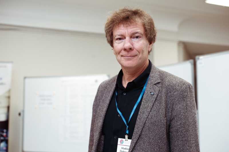
What are you and your colleagues from the Laboratory of Physics of Epitaxial Nanostructures working on right now?
I myself am a theoretical scientist and I model the growth and physical properties of semiconductor nanostructures. The key idea is to find out how, by controlling the growth of nanocrystals, we can change their temperature and material flow, resulting in the morphology, crystal structure, and other properties needed for specific applications.
In our work, we use the same traditional semiconductor materials used for lasers, light diodes, and telecommunications. These are the III-V semiconductors, which consist of atoms of elements in the third and fifth groups of Mendeleev’s periodic table – such as gallium arsenide, which was invented and first synthesized here in St. Petersburg.
We are attempting to create a nanomaterial that would improve the physical properties – efficiency, wavelength, and performance – of lasers, light diodes, photoreceptors, solar cells, and other devices widely used in everyday life.
Most of our work concerns the so-called nanowhiskers. They are tiny pillars of optoelectronic materials such as gallium arsenide, indium phosphide, etc. They are only several dozen nanometers in diameter, which makes it possible to grow them directly on the surface of silicon without causing any crystal defects, therefore creating electronic and optical systems integrated into a silicon-based electronic platform. In this manner, we integrate onto one chip what had been just a dream for thirty or forty years.
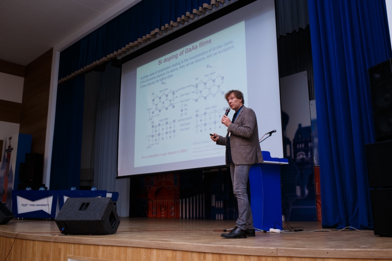
You’ve presented a report here at the Advanced Materials Week conference. Can you tell us a bit more about it?
Our section focuses on semiconductor nanomaterials for photonics, and most of the reports concern nanowhiskers. As for me, I spoke about the silicon-doping of gallium arsenide nanowhiskers. To create optoelectronics devices, you need a p-n junction; which means that one part of the semiconductor must have more electrons and the other must have less. When you connect such a structure to a battery and run a current through it, you get a semiconductor diode. But in order to create the p-n junction, we need to add atoms to the electrically neutral semiconductor in order to create more electrons or more “holes”. Silicon is a tetravalent element, gallium is trivalent, and arsenic is quintavalent. Therefore, silicon can serve as a replacement for either arsenic or gallium in gallium arsenide. And that results in either more electrons or more “holes”, depending on the conditions in which the crystal grows.
In my report, I presented a model and experimental results that show how we can control the type and level of silicon-doping of gallium arsenide semiconductor nanowhiskers, which can be controlled by modifying the material flows and temperature.
What would you say are the key tasks faced by nanophotonics scientists?
One of the tasks is to integrate photonics and electronics. Silicon does not work for most optoelectronic devices due to an internal quality – the so-called indirect-gap band structure. It cannot emit light effectively and therefore cannot be used to make lasers of light diodes, which require different kinds of material with a different crystal lattice. But if you try to grow them in the form of a thin film over a silicon surface, it just won’t work. The mechanical tension causes numerous defects or, simply put, fissures.
Our work is to make the nanostructures smaller and minimize the amount of contact with the silicon surface. That way, we can get rid of all defects altogether. Of course, that’s not our only goal.
Our general goal is to create new functional nanomaterials for specific applications, of which there are many. It’s everything related to photonics: lighting, data transfer and reception, and improved data security. To make things cheaper, lighter, and better, we must develop new functional devices, and that’s what we’re doing: making new nanomaterials that possess fundamental properties not found in other materials.
One of the talks, delivered by professor Jean-Christophe Harmand, concerned the observation of nanowhisker growth. In France, they’ve made this spectacular microscope inside which nanowhiskers are grown using molecular beam epitaxy. You can watch frame-by-frame, at atomic resolution, how these materials grow, complete with full diagnostics of the crystal lattice and chemical make-up. It’s a fascinating technology! If someone had told me 15 years ago that this was possible, I honestly wouldn’t believe them. This technology provides a lot of new material to consider for theoretical scientists. We must analyze what we’ve seen and answer new questions about the control of crystal lattices of these materials. Depending on the conditions, a cubic lattice may be transformed into a hexagonal one, resulting in the same material with different fundamental properties. We knew this could happen before, but now we know how to control that process.
You’re listed as a participant in almost every report of your section; other reports reference your work. Which is why I’d like to ask your opinion on how to develop international scientific collaboration. How does one make sure their team becomes a part of the general scientific community?
I don’t believe there is a universal recipe. It all starts with research; nobody’s going to work with you just like that. You start thinking by just reading articles. You create new pieces of knowledge, you publish your work. Preferably well-written in English and in good journals. Then, people come to you.
We were the first to release a series of studies on nanowhiskers in 2005. Our colleagues from France, whom we didn’t know, visited us after reading our work. We’ve been working together since. It’s important to set up international conferences, to take part in international events and projects. It’s just as important to exchange students. Essentially, you must not avoid cooperating with others; you have to analyze their data, their achievements, and to work alongside them.
How do you pick the Master’s and PhD students for your laboratory?
We give lectures. There’s a certain number of students who start to show interest. We involve those who study better and understand the subject well in our work; first, we help them, then they start doing things on their own. We were once picked that way, too, and now we do the same. The most important trait for a student who wants to join us is to love quietly and calmly doing research on their own.
Allow me to ask you a final, private question: what’s more important to you, awards and recognition or something practical made using your research?
The latter, of course. There was a time when we predicted that you can manipulate the crystal structure of gallium arsenide nanocrystals by changing the temperature. Researchers in France did an experiment where they increased the temperature by 100 degrees and caused a shift from cubic to hexagonal lattice. Bullseye! Two or three years later, people in Sweden began to produce superlattices based on crystalline phase interlacing. It’s an unusual heterostructure because the material is one and the same as opposed to the usual choice of different ones, but with a different crystal lattice. And these were used to introduce new types of single-photon emitters. That’s amazing.
