What It Does:
The “Functional Materials and Devices of Optoelectronics” laboratory is part of the International Research Center that studies the latest materials, including semiconductors, metals, and oxides in a nanostructured state, with the goal of using them in optoelectronics.
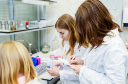
Students and employees of the laboratory study the properties of nanostructures and create new semiconductor devices for micro- and optoelectronics. The R&D find application in the field of energy-efficient LED lighting and will be in demand in the near future in high-voltage electronics of smart power grids.
In the student community, this lab on Lomonosova 9 is often called “The Romanov Laboratory”, since both the lab and the center are headed by Aleksey Romanov, Doctor of Science in Physics and Mathematics and Dean of ITMO University’s Faculty of Laser Photonics and Optoelectronics, the author of more than three hundred scientific publications and receiver of many international scientific grants and awards.
Equipment:
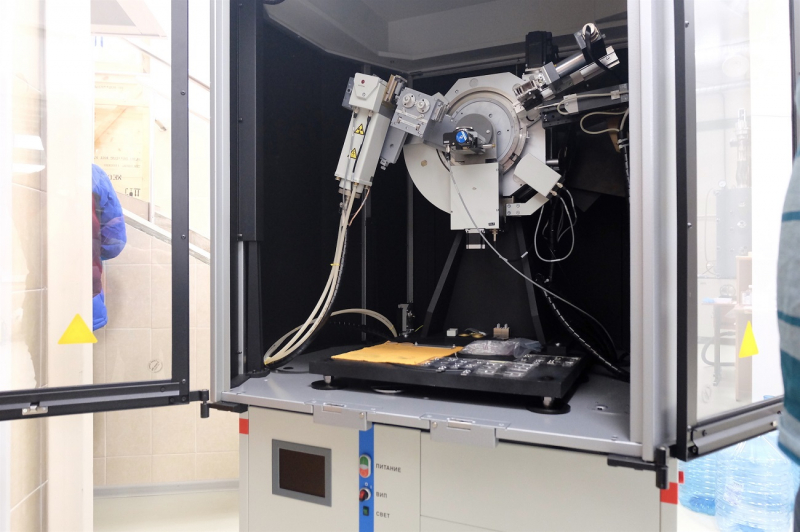
The lab is equipped with DRON-8 X-ray diffractometer by a Russian company Burevestnik. It is one of the main instruments for analyzing materials.
It helps characterize the quality of the obtained crystals and heterostructures by measuring the X-ray diffraction spectra. It is also used for heat treatment of the developed thin-film semiconductor structures.
We use modern semi-industrial systems to characterize, modify and sort LEDs. Let's talk about the first (in the photo below on the left side).
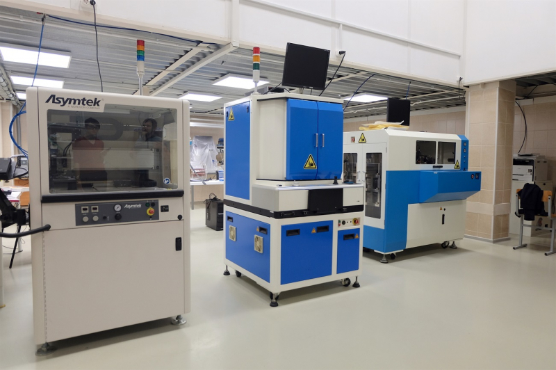
This is Asymtek S-820 precision dispenser. It is an automated system for dispensing viscous liquids. Such a dispenser is vital for accurately applying phosphor material to an LED chip in order to achieve the desired glow color.
The white LEDs we are used to are based on the chips emitting in the blue range of the visible spectrum of electromagnetic radiation.
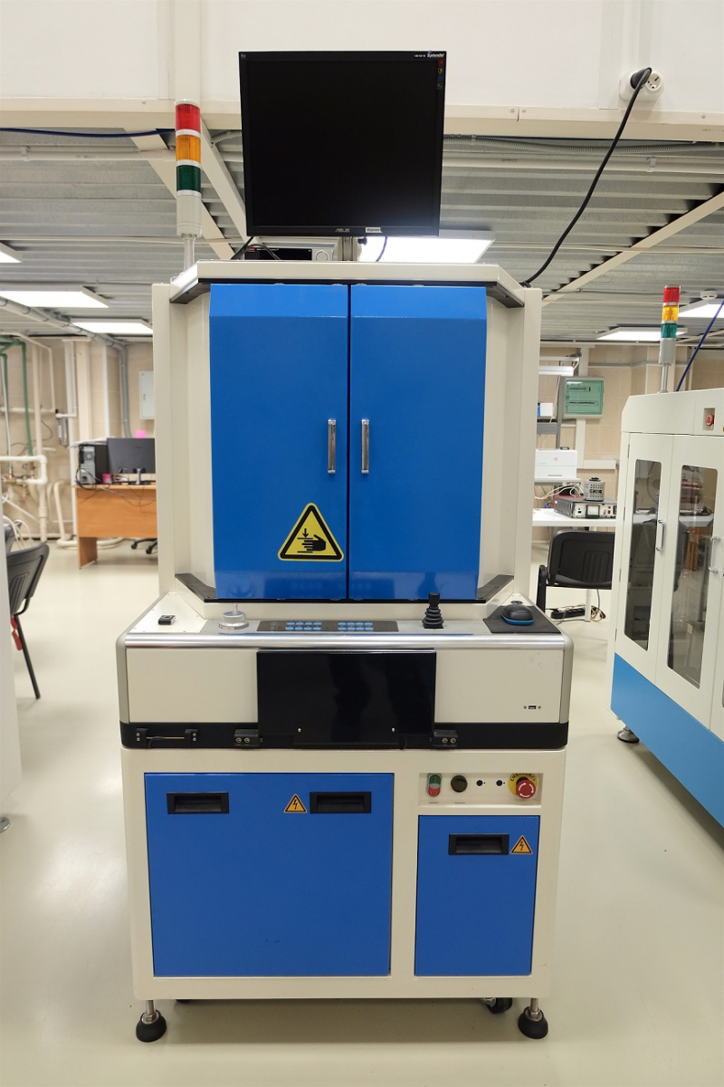
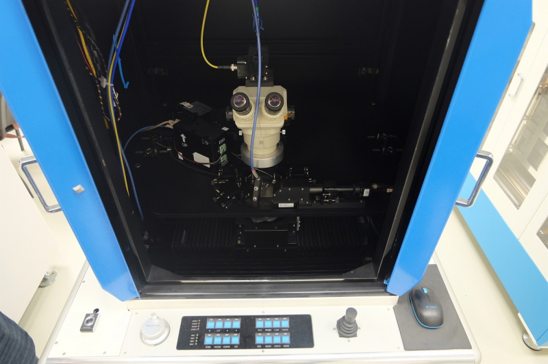
This device (in the center) measures the current-voltage and spectral characteristics of LED chips and stores the measured data for a large number of chips in the computer's memory. It is necessary to verify the electrical and optical parameters of the manufactured samples. This is what the device looks if you open the blue doors:
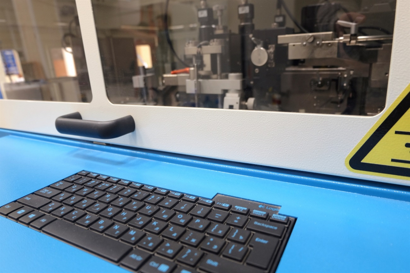
The third device in the photo is a system for sorting and preparing LEDs for subsequent installation. Based on the measured characteristics, it compiles a passport for the LED. After that, the sorter places it in one of 256 categories depending on the quality of the semiconductor device (category 1 - these are LEDs that do not glow, category 256 - those that glow most brightly in a given spectral range).
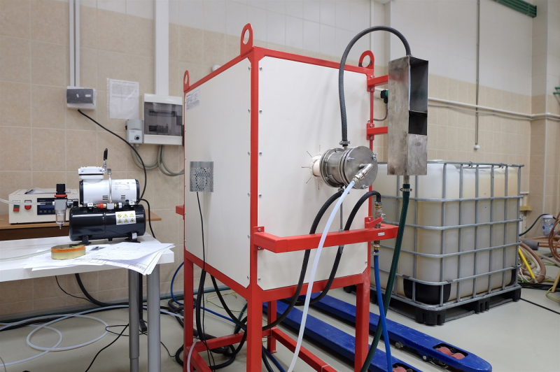
At our International Research Center, we also grow semiconductor materials and heterostructures. Heterostructures are grown by molecular beam epitaxy using the RIBER MBE 49 facility at Connector-Optics, a partner company.
To obtain oxide single crystals (which are wide-gap semiconductors) from the melt, we use the NIKA-3 multifunctional growth unit of domestic production. Wide-gap semiconductors can be used in power relays of the future, in high-performance VCSEL vertical lasers, in ultraviolet detectors, etc.
Projects:
Various fundamental and applied research is carried out in the International Research Center in our laboratory.
For example, together with researchers from Ufa State Aviation Technical University, we are developing new metal conductors with increased conductivity and strength using the methods of intense plastic deformation. The fine-grained structure of the alloy is subjected to heat treatment, redistributing the concentration of impurity atoms in the material. As a result, the conductivity parameters and strength characteristics of the material are improved.
Also, our staff are developing technologies for the manufacture of optoelectronic transceivers based on photonic integrated circuits. Such transceivers can be used for creating high-performance information transmission / reception systems. To date, a set of instructions is already prepared for the manufacture of models of radiation sources and photodetectors. Design documentation for testing them has also been prepared.
An important laboratory project is devoted to the creation of wide-gap semiconductor materials and nanostructures with a low density of defects. In the future, with the help of the developed materials, we will be able to produce energy-saving semiconductor devices that do not yet have counterparts in the market.
Our experts have already developed LEDs that can replace unsafe ultraviolet lamps based on mercury. The value of the manufactured devices is that the power of our ultraviolet LED assemblies is several times higher than the power of individual LEDs - 25 watts versus 3 watts. In the future, this technology will find application in healthcare, water treatment and other fields where ultraviolet is used.
A group of scientists from our International Research Center believes that future optoelectronic devices will use the remarkable properties of nanoscale objects - quantum dots with special optical parameters. Among them is the luminescence or non-thermal glow of the object, which is used in televisions, smartphones and other gadgets with displays.
We are already creating a new generation of optoelectronic devices. But, before the gadgets can enter the market, we have to work out the technology of materials production and confirm the safety of the materials for users.
Written by ITMO Media Office on Habr.