In this ITMO.NEWS interview he spoke in detail about the upcoming issue, the work on environmentally friendly materials for nanophotonics devices of the future, as well as what scientific news in recent years he was most surprised by.
To begin with, please tell us about the invitation you received from the editorial staff of Nanomaterials.
Today, the journal is on the rise – it’s turning ten years old, it has a relatively high impact factor, it’s in the first quartile of the material science section and in the second quartile of the nanoscience section (for more details about the quartile system, please refer to our interview with an expert from Clarivate Analytics). What’s more, these are open access publications, that is, their authors pay the editorial costs, and the readers can access these materials for free.
Recently, the editorial staff of the journal has asked me to become a guest editor of the special issue Electronic and Optical Properties of Nanostructures. The issue is now being compiled: I have sent invitations to the world’s leading scientists in the USA, Germany, France, Ireland, the UK, Japan, and Australia. I invite my colleagues from ITMO University and other Russian universities and scientific organizations to join me. The articles will be published as soon as they are received and reviewed, which generally takes about two weeks. Applications will be accepted until December 31.
What is the appeal of this issue for the international scientific community?
In recent decades, we have seen great success in the synthesis of different nanostructures – new structures create masses of different shapes and materials. Moreover, these nanostructures are increasingly being used as markers for sensors, detectors, optical radiation sources, and so on. Meanwhile, there is a lack of description of fundamental physical processes that form unusual optical properties of such nanostructures which in some cases makes it much more difficult to predict their electronic energy structure and optical properties.
Why do you think the editorial staff has approached you?
Our team has been working on nanostructures for many years, and I myself have been in this field since the 1990s. We have published hundreds of publications indexed in Scopus and Web of Science, and obtained over ten patents for inventions. Our center, together with a leading scientist and professor Yurii Gun’ko, has successfully carried out the mega-grant “Development of New Systems of Chiral Quantum Points and their Applications. And now we’re working with professor Andrey Rogach, who is also one of the leading specialists in the field, on the megagrant “Light Emitting Carbon Dots”.
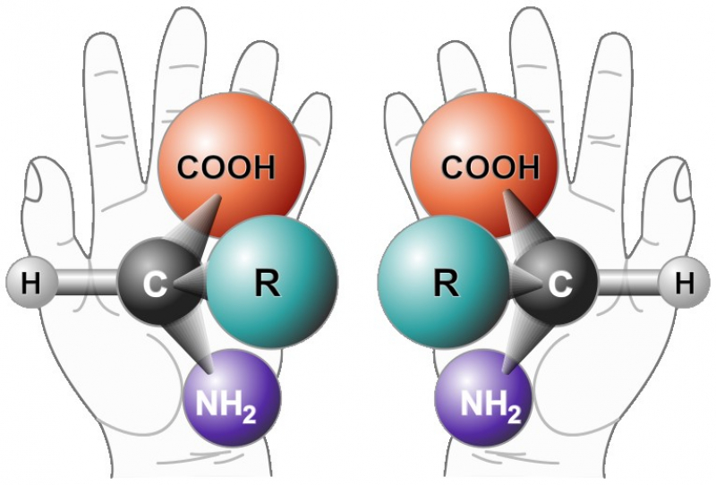
Together with Yurii Gun’ko, we have examined the optical properties of semiconductor nanocrystals. We have synthesized and researched new chiral nanostructures (the word “chiral” comes from the Greek χειρ – hand” – Ed.).
Chiral is an object which, like human hands, has no mirror symmetry and exists in two forms, which can be conventionally called “left” and “right”. Examples of such objects are sugar molecules, as well as active molecules of many drugs. The left and right molecules and nanostructures interact differently with the electromagnetic field, which can be used to create light emitters with right or left circular polarization.
It is also possible to create sensors for express drug analysis based on chiral nanostructures. As I said, a large number of drugs contains chiral molecules as an active substance, and one of their forms – left or right – can be useful, while the other does not have any effect or even causes harm. With our sensors, you can quickly test a new drug or generic for its usefulness.
Our second megagrant is dedicated to carbon dots. These are very interesting objects that are harmless to humans, and can emit light. Their basis can be used to build effective emitters for, say, monitors and TVs. This is a step towards “green” photonics because lead, mercury, arsenic and so on are not used here. However, there is a problem: carbon dots emit well in the blue and green areas of the spectrum, but they work much worse in the red and yellow ranges, and color images of screens are known to be formed from red, green and blue pixels. The goal of our project is to ensure that carbon dots emit well in the red and yellow parts of the spectrum.
We have a total of seven laboratories in our center – each has its own research areas. So we are dealing with a very wide range of nanomaterial related tasks. That’s probably what the editorial staff has noted.

You said that there is a misalignment between successful practice in creating nanomaterials and the fundamental physics that describes these processes. Why do theoretical scientists lag behind the practical part?
Today, chemists have learned to synthesize nanostructures in the form of quantum holes, quantum threads, spheres, parallelepipeds, rods, dumbbells, pyramids, tetrahedrons, tetrapods and even “colors” and “nano-matryoshkas”, where one structure is inside the other. In addition, more complex nano-objects have been created, consisting of the above-mentioned “elementary” structures. However, the description of most of them is related to very complex mathematics. In principle, quantum mechanics allows for solving any modern problems, but the cost is the main question.
The cost can be extremely high. A simple example from modern mathematics: there is the graph theory, which makes it possible to describe logistic systems. Imagine that you have drawn a graph which consists of n vertices connected by edges. You need to solve the so-called traveling salesman problem which means you have to build a path for traversing the edges of all the vertices in as little time as possible. If the number of vertices exceeds 60, even a modern supercomputer can search for a solution for trillions of years.

The physics of nanostructures has many such issues. The fact is that when studying nanostructures, it is necessary to take into account their real form. If we are talking about macroscopic objects, we often do not need to take their size into account, shape and surface condition, but for nanoobjects these parameters are very important. Therefore, we have the following situation: it is relatively easy to calculate analytically or numerically the key characteristics of a single atom, and to perform similar calculations for a system made up of an infinite number of atoms, e.g. a crystal (when we simply ignore the shape, size and state of the surface of a macroscopic body).
But it is extremely difficult to describe a system of several hundreds or thousands of atoms because analytical results can be obtained only for nanostructures with high spatial symmetry (sphere, cylinder, parallelepiped), and their numerical modeling, similar to the salesman problem, faces the problem of limited computational resources of modern supercomputers.

But is it so important if, as you said yourself, nanostructures are synthesized and technologists find applications for them?
That is the problem: applications are found, but how? For example, you have synthesized a new material and then you want to make a nanodevice based on it. For it to work optimally, you have to understand what kind of modifications to the material and the nanostructure you have to make, and it is very difficult to do that without fundamental theory. You have to go through an endless path of trial and error.
And what discoveries in the field of nanomaterials stood out to you in the recent years?
The latest was perhaps the synthesis of nanoplates, which was initially made by a group of international researchers based in France.
When you synthesize, for example, quantum dots, you get them in a slightly different size. Their size determines their absorption and luminescence spectrum. That is, if you take a glass of quantum dots, they will all be slightly different, and the absorption and luminescence spectrum will be different, so the whole glass will be very wide. This is called dimensional inhomogeneous widening of the optical spectra. Our French colleagues managed to synthesize very thin semiconductor wafers with thicknesses of 4, 5, 6, 7 and 8 monolayers. Now in our conventional “glass” there are nanoplates of the same thickness. The absorption and luminescence spectrum of such wafers is very narrow and there is no dimensional inhomogeneous widening.
Why is this important? For instance, to get a narrow line of laser radiation rather than a wide band. By the way, some time ago, in cooperation with German and Belarusian scientists, we contributed to the research on nanoplates and published in the ACS Nano journal, dedicated to the influence of an external electric field on their optical properties. Then a group of our theorists suggested an approach that allows us to design new nanoobjects, including nanoplates. Finally, we are currently working on the Russian Science Foundation project called “Near Infrared Radiation Sources based on Semiconductor Quantum Nanoplates”.
What are your expectations from the special issue that you are editing?
We will try to cover a wide range of nanostructures of various dimensions based on dielectric, semiconductor and metallic materials as well as their composites, including metamaterials. We would like to get a cross-section of the current state of affairs in the field of studying electronic and optical properties of nanostructures. It is extremely important that leading researchers take part in the special issue and identify in their work further areas of research development.
It would be great if young scientists, postgraduates, graduate and undergraduate students could take a look at it and see promising areas of research and understand what problems await their solution. It would be important and interesting.
Translated by Pavel Vorobyev