Owing to extremely high local field enhancement in metallic nanopores, plasmonic nanosponges are a powerful platform for various nanophotonic applications. The filling of the nanopores with high-refractive-index semiconductors (for example, Si, Ge, GaP, etc.) opens up opportunities for the enhancement of nonlinear effects in these materials. However, this task remains challenging due to the lack of knowledge on the integration process of metal and high-index semiconductor components in such nanoobjects.
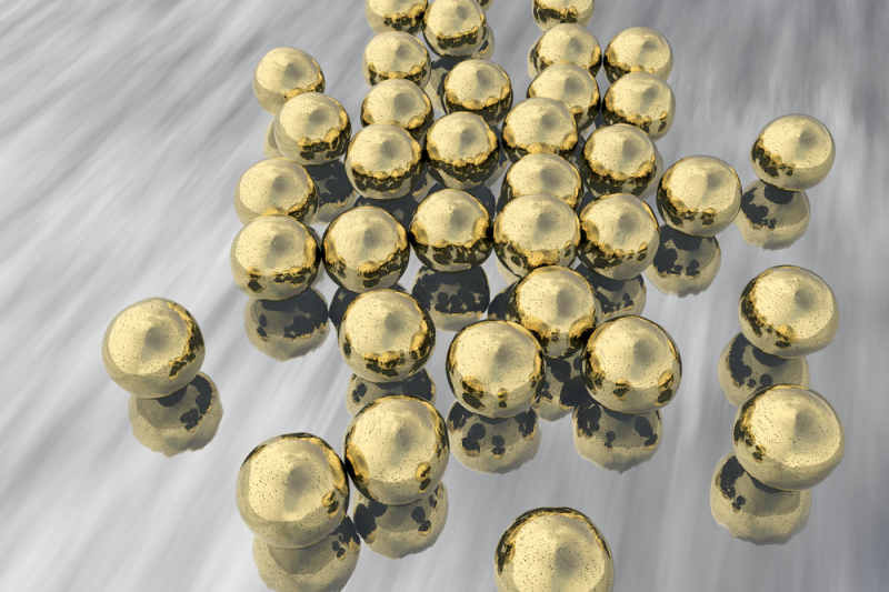
The researchers studied metal-dielectric nanostructures produced using the method of laser ablation of two-layer Si / Au films. Using a combination of theoretical and experimental methods, they found out that these hybrid nanostructures represented the Au sponge-like nanoparticle filled with Si nanocrystallites. They also demonstrated that the Au nanosponge provides strong near-field enhancement in the Si grains increasing the white light photoluminescence in the hybrid nanostructures compared to uniform Si nanoparticles.
These results pave the way for designing the internal structure of the sponge-like hybrid nanoparticles possessing white light luminescence and control of their optical properties on demand.
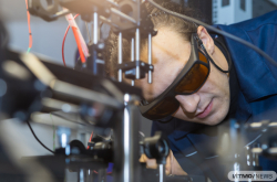
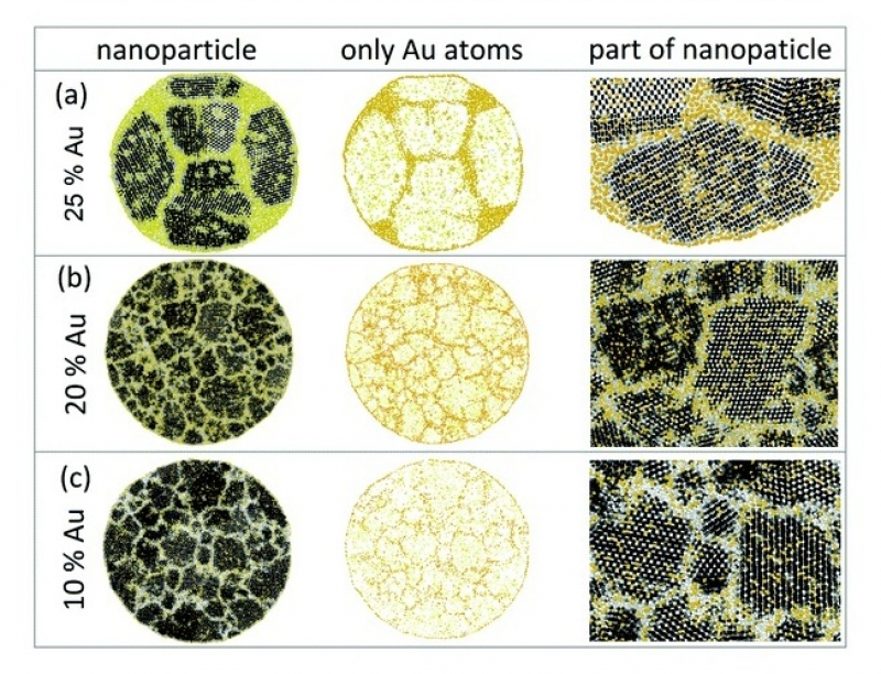
“It was Sergey Makarov, a PhD in Physics and Mathematics, who started working on this project. Together with his team, he performed the synthesis of this nanostructure and revealed that it was silicon that was the source of its radiation. Though it isn’t a direct-gap semiconductor and its optical transitions are very insignificant, with a quantum efficiency of about 10-5, in this structure silicon starts to radiate and its quantum efficiency increases multifold – up to 0.1%. My part of the work consisted of carrying out additional measurements of the structure’s nonlinear optical properties at maximum excitation powers, as well as conducting numerical simulations to demonstrate how this structure can amplify radiation over a wide wavelength range, why we can use different radiation pump lengths, and how this is related to the structure’s resonance properties. In their turn, my colleagues produced a simulation of how silicon and gold atoms would be distributed at the nanoscale with different variations in the degree of cooling, and also developed images from a transmission electron microscope, obtaining a real image of our nanostructures in cross section,” explained Artem Larin, ITMO University PhD student and one of the authors of the article.

He also added that going forward, he plans to go to the University of Lorraine (Nancy, France) to continue the research in order to find out how this structure will change, geometry-wise, during thermal annealing.
The hybrid particles obtained can be applied in broadband near-field microscopy. The topicality of the research is further confirmed by the fact that though broadband near-field microscopy does exist at present, it necessitates every-time excitation of the radiation in the near field, and only then its detection in the far-field. Thus, existing approaches only allow scientists to work in a very narrow range of excitation wavelengths, and changing it requires a full equipment readjustment. The proposed hybrid nanostructure will allow for circumventing this requirement, simultaneously working at different wavelengths. This can reduce equipment costs and save researchers time.
Reference: A. O. Larin, A. Nominé, E. I. Ageev, J. Ghanbaja, L. N. Kolotova, S. V. Starikov, S. Bruyère, T. Belmonte, S. V. Makarov and D. A. Zuev, “Plasmonic nanosponges filled with silicon for enhanced white light emission”, Nanoscale.