Frontier laboratories are brand-new departments of ITMO University that are going to be engaged in research at the scientific frontier. Their main goal is to consolidate efforts in order to achieve breakthrough results and fundamental discoveries that will change the way we see the world or provide a foundation for technologies of the future.
These goals are a part of ITMO’s 2030 Development Strategy and will be implemented as part of the Scientific Breakthrough strategic project. The plan is to launch at least 10 frontier laboratories by 2024. In 2021, the first open call for such projects was held.
The selection process was quite rigorous: project heads need to have proven their experience of working at the frontier of science, have publications in the top 3% of the world’s most-cited journals, undergo a review process, and find supporting experts, as well as form a team that includes young specialists and students.
As a result of the competition, six frontier labs will be created in the nearest future:
-
Infochemistry Scientific Center, headed by Ekaterina Skorb
-
Laboratory “Computational Methods for Systems Biology”, headed by Alexey Sergushichev
-
Laboratory “Frontier Nucleic Acid Technologies in Gene Therapy of Cancer”, headed by Daria Nedorezova
-
Laboratory “Probing Fundamental Physics with Topological Metamaterials”, headed by Maxim Gorlach
-
Laboratory “Functional Materials for Polaritonic Quantum Logic”, headed by Ivan Iorsh
-
Laboratory “Solution-Processable Laser Diodes”, headed by Sergey Makarov
The latter three labs will be established at ITMO’s School of Physics and Engineering. We asked their heads to share what they are going to research and what results they plan to achieve.
Maxim Gorlach
Senior research associate at the School of Physics and Engineering, head of the Laboratory of Probing Fundamental Physics with Topological Metamaterials
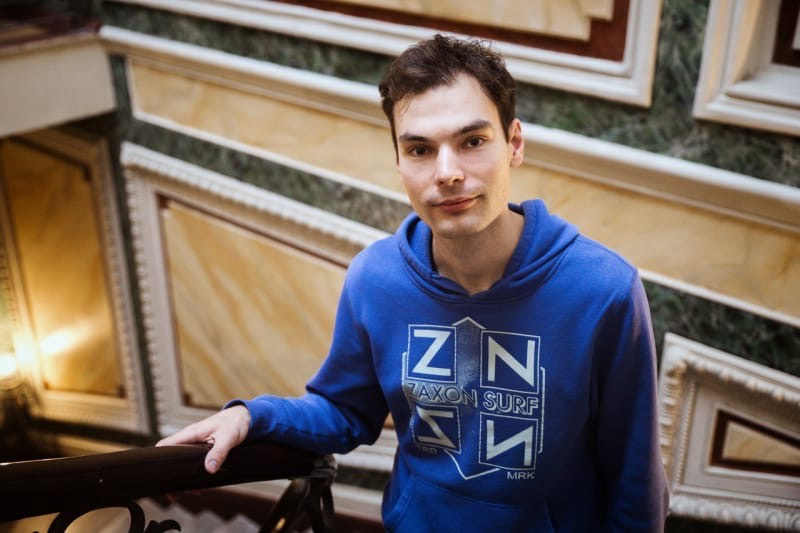
Maxim Gorlach. Credit: ITMO.NEWS
Project concept
Back in the 1930s, astronomers discovered that there is not enough matter registered in the universe using optical methods to explain the motion of stars and galaxy clusters. Therefore, they had to hypothesize the existence of dark matter, which participates in gravitational interaction, but practically does not manifest itself electromagnetically. The mystery of dark matter has not been solved yet. Those who will get to the bottom of it will most likely receive the Nobel Prize. There are various theories on what the dark matter particles are, but many of them have already been disproven. Scientists now believe that the most promising candidate is the hypothetical axion particle, first suggested in the 1970s.
Recently, Professor Frank Wilczek, the 2004 Nobel laureate in physics, and his co-authors came up with a promising way of experimental detection of axions using metamaterials. This initiative led his team to cooperate with the staff of the ITMO’s School of Physics and Engineering – largely due to our accumulated competencies in the physics of metamaterials.
While the search for cosmic axions is an extremely ambitious task with no guarantee of success, similar equations of axion electrodynamics are also found in condensed matter physics. Elementary collective excitations (quasiparticles) have all the properties of an axion and serve as a kind of testing ground for the detection of cosmic axions. So-called axion topological insulators are promising structures of this kind.
When discussing our cooperation with Prof. Wilczek, we found out that axion topological insulators have just been implemented in condensed matter physics. At the same time, both the creation and the experimental research of such structures are very laborious. However, axionic topological insulators have not yet been implemented in photonics, and they may turn out to be much more accessible for experiments. That’s the task that lies in front of us.
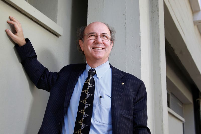
Prof. Wilczek. Credit: metode.org
Expected results
Among the expected quick wins of this project is the creation of 3D topological insulators that will serve as a starting point for the creation of axion topological structures. We plan to implement such structures in the microwave range at gigahertz frequencies – this helps make the development and experimental research much easier.
We would like to note that this field is new to us and we have a lot to learn. We actively look for new team members among Bachelor’s, Master’s, PhD, and postdoc students. Among the main advantages of participating in this project is the opportunity to work with Prof. Wilczek, a Nobel prize laureate, and learn about cutting-edge practices from the world’s leading researchers. And we’re already not wasting any time: in a few weeks, my PhD student, who’s visiting the US through the Fulbright program, will conduct a seminar on this topic at MIT.
Other than that, we will launch an optional course in September 2022. It will be available to fourth-year Bachelor’s, Master’s, and PhD students and educate them on the physics of topological insulators. We will also share our results at various open scientific seminars and promote them not only in academic media, but on social media, too.
We hope that our team’s work will not only result in scientific achievements but also help kick-start the careers of young scientists working on the scientific frontier.
Ivan Iorsh
Chief research associate at the School of Physics and Engineering, head of the Laboratory of Functional Materials for Polaritonic Quantum Logic
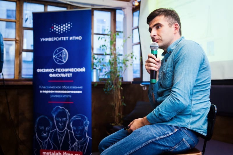
Ivan Iorsh. Credit: ITMO.NEWS
Project concept
Typically, the laws of quantum physics work on the micro-scale – at the level of single atoms or nanoparticles. But there is a whole class of materials which don’t abide by the laws of classical physics even on a bigger scale. A superconductor is the most obvious example. If you cool mercury down to a certain degree, the resistance inside of it completely disappears and the entire system can be described by one wave function as if it contains only one atom.
There are many materials of such kind – they’re called quantum materials. Their quantum properties are caused by the fact that the movement of electrons in such systems is correlated, unlike in other materials where the electrons move independently. This phenomenon leads to the appearance of new phases of matter, such as hyperconductivity.
Usually, the process of creating quantum materials is technologically very complex and expensive. In fact, it can be compared to alchemy: you need to spend a lot of time selecting elements, combining them into complex structures, and making calculations. At least this was the case before graphene, a simple material: it consists of an atom-thick layer of carbon packed into a honeycomb-shaped cell.
For our project, we take as a basis the key research in the field of quantum materials of the last two-three years. We will focus not on graphene but other materials – two-dimensional semiconductors. This is a class of materials that consist of one atom of a transition metal (molybdenum, tungsten, or rhenium) and two chalcogen atoms (selenium, sulfur, or tellurium). Such materials have fairly stable configurations in the form of two-dimensional films only one atom thick. Their properties allow us to investigate them optically and, moreover, they can be controlled using laser radiation. We will study the emergence of the quantum nature of materials in folded structures, which are monoatomic layers of two-dimensional semiconductors.
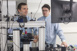
School of Physics and Engineering's International Laboratory of plant neurobiology of Light-Matter Coupling in Nanostructures. Credit: Dmitry Grigoryev, ITMO.NEWS
Expected results
Our goal is to demonstrate that it’s possible to control quantum states of substances optically. This has actually already been implemented in cold atom gratings: atoms are cooled down to mere thousandths of a degree above absolute zero, placed in an absolute vacuum, and are irradiated by ten lasers at the same time. But this costs millions of dollars and even though it’s an important fundamental achievement, it won’t become a commonplace technology. We would like to achieve a similar level of control but in a way that would be useful for quantum computers and sensors – one that works with a small solid-body device or a chip. This would be a fantastic result.
We’ve been engaged in two-dimensional semiconductors for the past four years as part of a megagrant project. We have theoretical and experimental experience with two-dimensional materials, but folded layers are new to us.
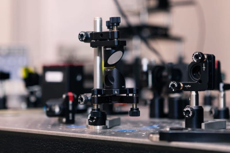
We’ll need some optical equipment, particularly some systems for counting single photons – those are the systems through which it’s possible to determine whether correlated phases appear in matter or not. The frontier lab program will help us a lot because we will be able, firstly, to focus on our task, and secondly, to make necessary upgrades to our installations.
Sergey Makarov
Chief research associate at the School of Physics and Engineering, head of the Laboratory of Solution-Processable Laser Diodes
Sergey Makarov. Credit: ITMO's School of Physics and Engineering.
Project concept
Our project is more fundamental than technological, but it’s not limited only to the knowledge of basic laws of nature. We think that the result will lie in the creation of a preliminary prototype – a laser diode based on materials and nanomaterials obtained by the methods of solution chemistry that could work thanks to electric pumping. This task hasn’t been solved yet.
The first Nobel Prize in this field was awarded for the invention of lasers to two of our compatriots – Nikolai Basov and Alexander Prokhorov. By the way, I worked in the laboratory founded by Basov in Moscow, wrote my PhD thesis there, and saw one of the first laser installations in the world. I felt inspired working in the place where one of the most striking breakthroughs in 20th-century physics was made. In 2000, the Russian scientist Zhores Alferov received the Nobel Prize for the creation of heterostructures, which led to the appearance of semiconductor lasers – this was a bit similar to our project, but in that case they used solid-state technologies, which require the highest-quality materials, special application conditions, and expensive installations.
The next step for us is the creation of lasers from materials that can be obtained in a test tube. The materials we are currently working on – perovskites and semiconductor nanocrystals – can be dissolved in a liquid and applied in solution layers to any surface. At the same time, due to simple chemical reactions, perovskites can be given any color of radiation: near-ultraviolet, visible, or near-infrared. Moreover, synthesizing materials as nanocrystals makes it possible to control the band gap due to the quantum size effect. That is, by controlling the composition of the material and the size of the nanocrystals, we can achieve the required parameters in terms of the radiation wavelength and, ideally, obtain the maximum efficiency of light emission.
We expect that such laser diodes will be much cheaper and suitable for the implementation of flexible devices, that is, they could be built into clothing or wearable devices. In addition, we see great potential for this technology in devices for human health monitoring – for example, in pulse oximeters that have been seeing wide use during the pandemic. We already have some groundwork in this area, although not with lasers but with LEDs. However, I think that while working on these fundamental and applied tasks at the same time, we will eventually be able to create a working prototype.
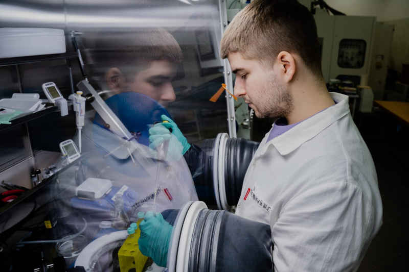
ITMO's Laboratory of Hybrid Nanophotonics and Optoelectronics. Credit: ITMO.NEWS
Expected results
We have set ourselves a very ambitious goal. Dozens of laboratories all over the world are working on this challenge, but so far laser diodes of this kind haven’t been implemented anywhere. This is inspiring, although we are aware that there are still many problems to be solved. However, we have some advantages over other laboratories: we are already capable of making excellent optically pumped lasers, synthesizing new laser nanomaterials, implementing multilayer architectures for electrically pumped devices, and we also have excellent groundwork in the field of ultra-compact resonators.
Our team consists of 18 people and more than half of them are students. The average age of our members is less than 30 – about one student per one PhD. Moreover, we will work in close collaboration with such prominent scientists as Yuri Kivshar, Andrey Rogach, Anvar Zakhidov, and Volkan Demir. Thus, young researchers will write their theses based on world-class results and gain experience in international cooperation.
This is another important task to be solved by our lab – to foster a new generation of interdisciplinary researchers. I think it’s a perfect model for scientific activities because students will know that their results are real and valuable.