Countless counterfeit products are being made in the world. According to a study (in Russian) conducted by the Eurasian Economic Commission, the total loss made by selling such products will reach almost $5 billion by 2022. Almost any product can be counterfeited: expensive watches, household appliances, clothes, food, and medicine.
“According to the World Health Organization, about 10% of all produced drugs are counterfeit – and that’s a huge problem,” explains Dmitriy Zuev, assistant professor at ITMO’s Faculty of Physics and Engineering. “In poor countries, such drugs cause a large number of deaths.”

It’s no wonder that companies all over the world are looking for new opportunities to more securely protect their products from forgery. New tools are appearing: QR codes, stickers, protective labels, and holograms. But all of these are only temporary solutions. As soon as a new protection method is introduced, criminals are starting to look for ways to imitate it. Thus, manufacturers have to constantly come up with more complex ways to keep the criminals at bay and protect their goods.
Silicon labels
Scientists from ITMO together with their collaborators from St. Petersburg Academic University, the Institute of Automation and Control Processes of the Far Eastern Branch of the Russian Academy of Sciences, and Far Eastern Federal University suggested a new protective label to identify authentic goods. It is created from a semiconductor material with the help of a laser. At the same time, its authenticity can only be verified with special equipment.
“We used an electric beam to warm up silicon in a high vacuum chamber. After some time, silicon molecules settled on the substrate in a thin layer. Then, with the same method we fabricate a layer of erbium for later introductions of erbium alloys,” says Lilia Dvoretckaia, junior researcher at St. Petersburg Academic University.

The acquired two-layer films were used as the basis for subsequent recording of the protective label by laser radiation.
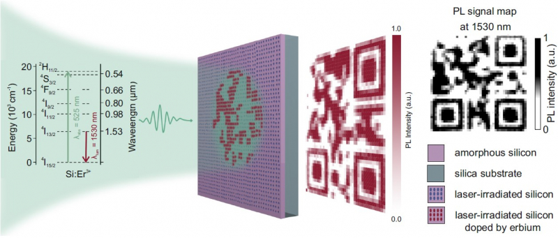
“In this project, we used thin film silicon structures that we locally enriched with ions of a rare-earth metal, erbium,” comments Artem Larin, first author of the paper and a PhD student at ITMO’s Faculty of Physics and Engineering. “These ions integrate into silicon when subjected to laser radiation. Simply put, laser processing creates a pattern of microholes that contain a luminescent material.”
Creating a pattern using erbium ions, however, is only the first step. After that, a multitude of holes that do not contain erbium is created in the sample.
“If we look at the sample using a microscope, we will see a pattern of holes that are visually indistinguishable from each other,” adds Dmitriy Zuev. “But if we shine a green laser on them, then certain holes start luminescing in the infrared wavelength region (invisible to the human eye). At the same time, the luminescent spectrum is unique to erbium. These holes form an image that we record as a protective label and then additionally mask using a separate layer of non-luminescing (confusing) holes.”

How it works
It is impossible to see such an image with a naked eye. For that, you will need a green laser and an infrared detector, so this system is meant to serve large storage facilities and logistic centers, which face counterfeit, have need to battle it, and thus are ready to invest in relevant fields.
Thanks to such precautions, wrongdoers won’t be able to see the image on the label. In order to do that, they would have to get into the shipment system, learn to work the equipment, and master label reading methods. These labels are made even more secure due to several customizable characteristics.

“Our labels are based on erbium ion luminescence, which is characterized by several parameters: intensity, wavelength, and radiative lifetime,” says Artem Larin. “A combination of these parameters allows us to create additional layers of protection. That’s why when you get the hidden image with an infrared sensor, you will also be able to read the information about the luminescence parameters. This provides an additional degree of protection .”
At the same time, the new labels are resistant to chemical and physical effects, durable, and allow for multiple readings. “Such labels can potentially be formed on flexible substrates, which raises the appeal of integrating them into the real economy sector,” comments Ivan Mukhin, head of a laboratory at St. Petersburg Academic University and a researcher at ITMO.
The investigations are supported by grants of the Russian Foundation for Basic Research (18-29-20107 мк) and the Russian Science Foundation (19-19-00691).
Reference: Artem O. Larin, Liliia N. Dvoretckaia, Alexey M. Mozharov, Ivan S. Mukhin, Artem B. Cherepakhin, Ivan I. Shishkin, Eduard I. Ageev, Dmitry A. Zuev Luminescent Erbium‐Doped Silicon Thin Films for Advanced Anti‐Counterfeit Labels. Advanced Materials, 2021/10.1002/adma.202005886


