Copper is a great conductor of electricity, which is why it is often used in electronics: for instance, in motherboards or printed circuit boards found in devices we use on a daily basis: computers, smartphones, washing machines, and others.
In order for motherboards and printed circuit boards to conduct electricity, their surface is covered with several conductive micropatterns that are connected to each other and the board’s other elements. The patterns themselves can be created via several methods, such as lithography – a deep printing technique wherein the pattern is transferred from one coil to another and then electrically deposited. However, all of these methods aren’t ideal. For instance, lithography requires a thorough preparation and is itself time-consuming: it takes around 40 hours to create a pattern. As for the other two methods, both of them require expensive equipment and large quantities of solvents in order to cover the material with a copper layer. All of this isn’t economically beneficial for small-batch production. Moreover, these methods limit manufacturers in the combinations of surface materials and metals used in printing – in different combinations, these materials have different adhesive properties. In order to solve this problem, additional laborious and time-consuming preparations have to be performed.
All of these challenges can be overcome with laser processing, such as direct laser writing of micropatterns on the surface or inside glass and consecutive chemical deposition. These methods have been developing since the 1970s and have already demonstrated their advantages: they are faster, more environmentally-friendly, and efficient, as well as flexible in terms of the micropattern that can be used. However, even here there are caveats: an expensive femtosecond laser is required for direct laser recording. Moreover, its work can be destabilized by external conditions. Finally, laser chemical deposition means toxic and expensive solvents.
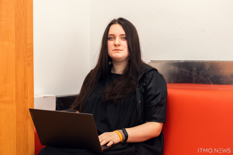
Ekaterina Avilova. Photo by Dmitry Grigoryev, ITMO.NEWS
Researchers from ITMO’s International Laboratory "Laser Micro- and Nanotechnologies," SCAMT Institute, and the Institute of Chemistry of St. Petersburg State University have developed a new laser-induced copper deposition method from deep eutectic solvents that combines the advantages of the existing methods. At the same time, the scientists were able to make the printing process cheaper and quicker. The respective study has shown the pattern-forming speed to be over 100 times faster than in earlier studies.
“A restoring reaction lies at the basis of laser-induced copper deposition. Thanks to high temperatures and wide gradients (meaning that we can quickly heat up and cool down the micropattern), laser radiation allows us to initiate processing and the restoring reaction faster. Moreover, the laser allows us to create any pattern: we only have to set the specific parameters and draw the laser’s trajectory in Adobe Photoshop or similar software,” says Ekaterina Avilova, the paper’s first author, a researcher at ITMO’s International Laboratory "Laser Micro- and Nanotechnologies," and a second-year Master’s student.
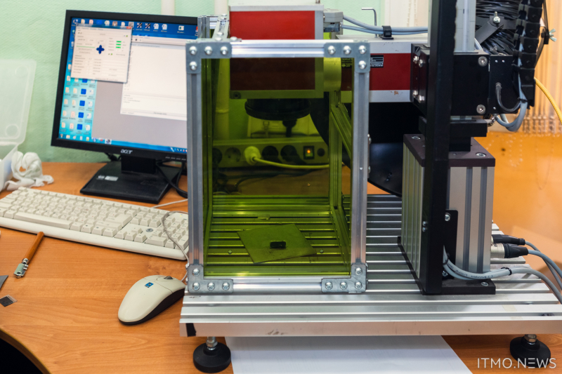
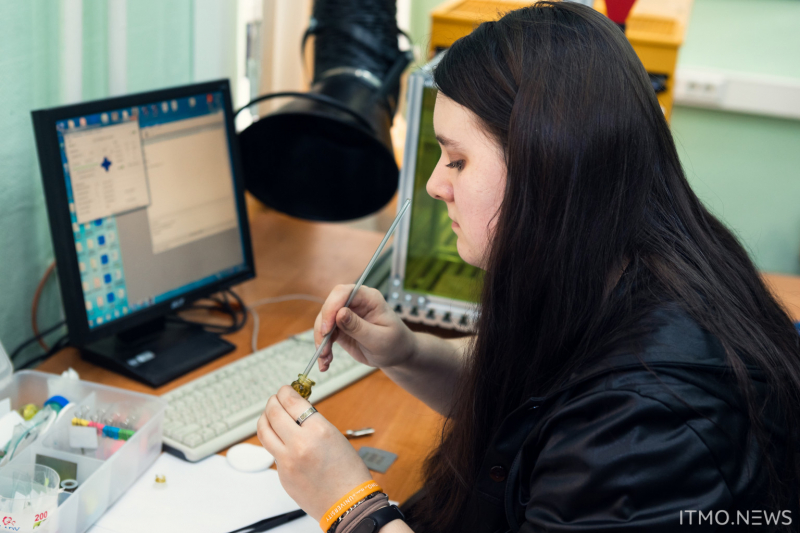
Inside the laser-proof protective box, the glass is put on a titanium plate and then treated with laser-generated plasma from one side. As a result, a layer of auxiliary particles forms on the surface, increasing its adhesion. Photo by Dmitry Grigoryev, ITMO.NEWS
Inside the laser-proof protective box, the glass is put on a titanium plate and then treated with laser-generated plasma from one side. As a result, a layer of auxiliary particles forms on the surface, increasing its adhesion. Photo by Dmitry Grigoryev, ITMO.NEWS
Inside the laser-proof protective box, the glass is put on a titanium plate and then treated with laser-generated plasma from one side. As a result, a layer of auxiliary particles forms on the surface, increasing its adhesion. Photo by Dmitry Grigoryev, ITMO.NEWS
Inside the laser-proof protective box, the glass is put on a titanium plate and then treated with laser-generated plasma from one side. As a result, a layer of auxiliary particles forms on the surface, increasing its adhesion. Photo by Dmitry Grigoryev, ITMO.NEWS
A “sandwich” under laser radiation
The writing of micropatterns is done in several stages. First, the researchers clean a glass surface from dirt, dust, and fingerprints, because any residue left on the surface can affect the following chemical processes, as well as the interaction of the laser and the surface. Then, the laser-induced microplasma technique is used to prepare the surface. This means that the glass is put on a titanium plate and then processed with plasma generated by laser radiation. As a result, a dark patina is created from titanium’s combustion products and oxides in the form of small particles that produce additional crystallization centers. In their turn, they absorb radiation thus supporting the necessary temperature. Additionally, this process changes the glass surface increasing its adhesion.
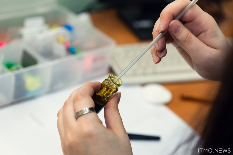
After that, a deep eutectic solvent made from tartaric acid, copper acetate, and choline chloride, with the latter responsible for the solvent’s consistency, is put on the glass. This composition of the solvent is cheaper and more environmentally-friendly; moreover, it is able to quickly decompose metal salts in high concentrations in a higher temperature. This is necessary for more efficient synthesis of electric wires from copper on glass. At the same time, the deep eutectic solvent can be stored longer and used more sparingly compared to its organic and water-based counterparts.
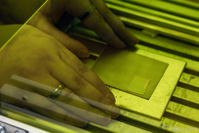
A deep eutectic solvent is applied onto the plasma-treated glass; then, copper micropatterns are synthesized from the solvent through a restoring reaction. Next, another layer of glass is put over the solvent. The resulting “sandwich” is subjected to laser radiation to shape a conductive micropattern. Photo by Dmitry Grigoryev, ITMO.NEWS
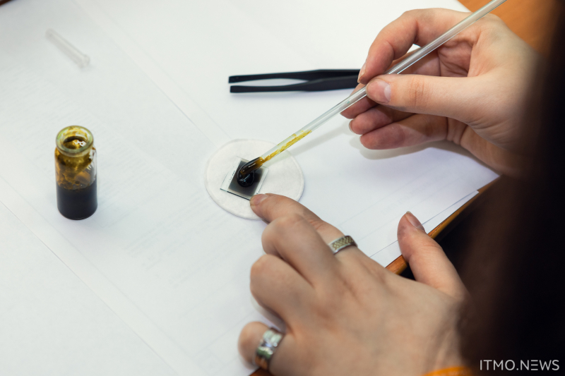
A deep eutectic solvent is applied onto the plasma-treated glass; then, copper micropatterns are synthesized from the solvent through a restoring reaction. Next, another layer of glass is put over the solvent. The resulting “sandwich” is subjected to laser radiation to shape a conductive micropattern. Photo by Dmitry Grigoryev, ITMO.NEWS
At the next step, another layer of glass is put over the solvent-lubricated surface in order to get rid of air bubbles, allow the solvent to spread more evenly, and keep it inside the processing area. When subjected to high temperatures and laser radiation, the solvent thickens, thus triggering the so-called Noah effect, which is when the liquid spreads from the center of the glass to its edges. The researchers have nicknamed this design a sandwich.
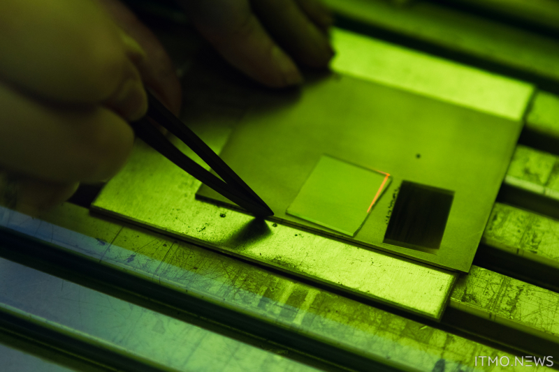
Finally, at the last stage the “sandwich” is once again subjected to laser radiation, forming on the lower glass the micropatterns previously designed using graphic software. They can take any shape depending on the researchers’ current plan: for instance, circles and lines for SPEs (screen printed electrodes) or complex shapes with many angles for multifunctional sensors.
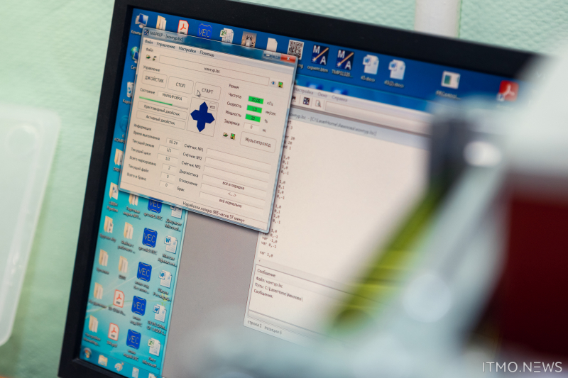
The chosen design, as well as the necessary printing parameters (velocity, radiation power, distance between lines, etc.) can be set in SinMark or MaxiGraf software. One of the possible designs is a square gear. Photo by Dmitry Grigoryev, ITMO.NEWS
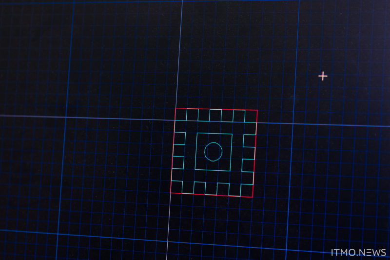
The chosen design, as well as the necessary printing parameters (velocity, radiation power, distance between lines, etc.) can be set in SinMark or MaxiGraf software. One of the possible designs is a square gear. Photo by Dmitry Grigoryev, ITMO.NEWS
Flexible electronics, sensors, and more
The new method can be used in different fields – for one, in the development of chemical sensors. These devices react to changes in the contents and volume of components in a chemical environment. Moreover, the method can be used to create RFID markings, a common theft-prevention technology. As the new method allows to create very complex outlines, this will make it possible to conclusively tell which brand store the item was taken from. However, according to the researchers, it’s not the only application.
“Any electronic circuit board with a worn-off pattern is usually disposed of; however, our method will allow us to refurbish it by recording it once more. We are also hoping that our method will prove useful for flexible electronics, because our technique can be used to design flexible screens or physiological sensors that are stuck on the body to measure the body’s water balance or level of sugar. This design can be helpful in treating diabetes,” adds Ekaterina Avilova.
In the near future, the team is planning to improve the method with the help of several scientific groups. In this interdisciplinary study, chemists will be responsible for adjusting components’ concentration or replacing components to see how it affects the method's efficiency. At the same time, physicists will study the laser radiation properties, such as power, frequency, and wavelength. It is also important to take into account the various aspects of pattern-writing: from the distance between its lines to the writing sequence, number of treatments, and so on. All of this will help the scientists increase the speed of micropattern formation and increase its quality.
Apart from that, the research team is planning to experiment with laser writing modes and surface material. The former is needed to increase the printing’s efficiency, while the latter will improve the technological applicability of the method. Using such materials as polyimide or fiberglass will make it possible to offer more options to the market.
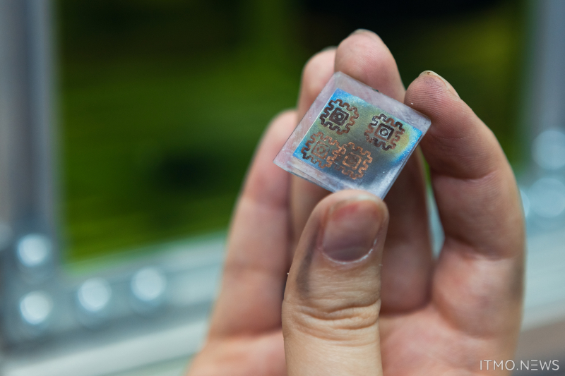
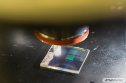
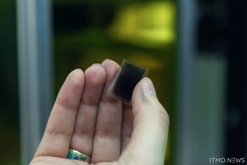
The result of laser printing: a square gear and an SPE element fragment. Photo by Dmitry Grigoryev, ITMO.NEWS
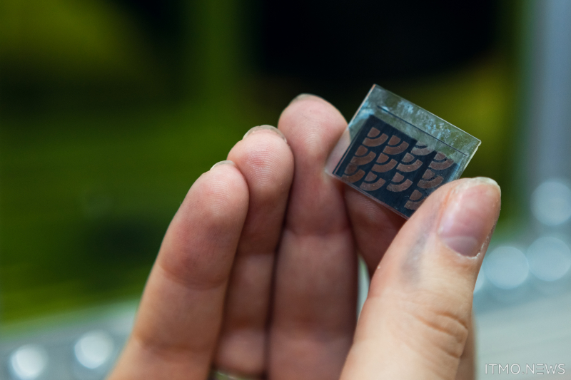
The result of laser printing: a square gear and an SPE element fragment. Photo by Dmitry Grigoryev, ITMO.NEWS
This project was supported by the Russian Science Foundation (projects No. 20-79-10075 and No. 21-79-1024), as well as an R&D grant for Bachelor’s, Master’s, and PhD students at ITMO University’s School of Physics and Engineering.
Reference: Ekaterina Avilova, Evgeniia Khairullina, Andrey Shishov, Elizaveta Eltysheva, Vladimir Mikhailovskii, Dmitry Sinev and Ilya Tumkin, Direct Laser Writing of Copper Micropatterns from Deep Eutectic Solvents Using Pulsed near-IR Radiation (Nanomaterials, 2022).