Every year, new electronic devices emerge on the market. Their power and functionality can be increased with faster, more energy-efficient components capable of storing more data. However, improving these properties inevitably leads to an increase in their size, which isn’t convenient for users. That’s why miniaturization becomes a crucial problem to solve. One possible solution is to use new types of structures and active 2D materials.
Currently, some of the most promising structures are 2D crystals based on metal-organic frameworks (MOFs), wherein organic molecules are bound to each other by metal ions, producing a durable material with organic properties. Such structures can act as conductors or dielectrics by changing their conductivity with the help of an external electric field.
However, in their initial form, the majority of MOFs are 3D crystals – and scaling them for nanoelectronics devices is a complicated process. Researchers from ITMO University have suggested a technology for turning 3D structures into 2D ones that can be easily integrated into existing nanoelectronics devices. The team has discovered that when synthesized with certain organic compounds (ligands), 3D structures will disassemble into 2D ones unprompted. The resulting 2D structures demonstrate improved electronic properties compared to their 3D counterparts.
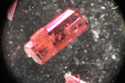
Crystalline structure. Photo by Dmitry Grigoryev / ITMO NEWS
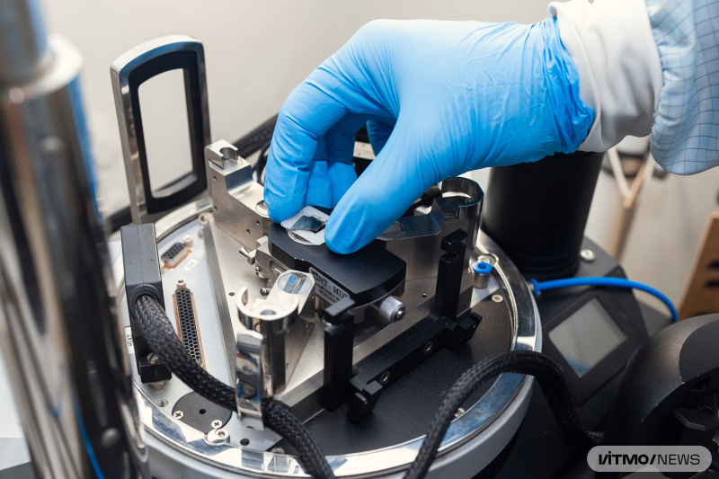
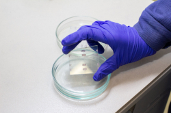
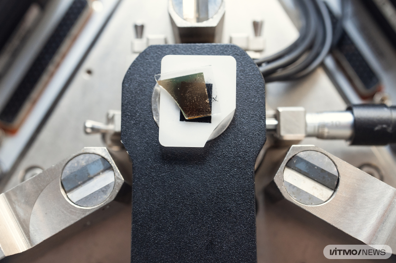
Photo by Dmitry Grigoryev / ITMO NEWS
First, the scientists synthesize 3D crystals. For this, they heat up a solution containing 1,2-bipyridyl ethylene, 2,6-naphthalenedicarboxylate, and zinc nitrate for 48 hours. The required structures precipitate in the sediment of this mixture. Once the crystals are separated from the solution, they are dried for 10 minutes at 40°C to evaporate the solvent and break the bonds between the layers permanently. In the final stage, the researchers use a special adhesive tape to separate the resulting 2D crystals. These layers can then be processed individually and used in various devices.
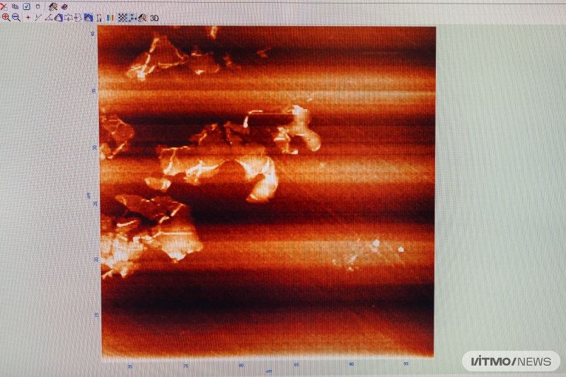
“A single 3D crystal can contain up to ten separate layers, which means that once the 3D structure of one crystal is destroyed, we acquire several 2D crystals. Such experiments were conducted before, but no one demonstrated that structures can disassemble unprompted, in the air. This makes their production significantly simpler and cheaper. At the same time, with our method, it’s possible to create structures with the necessary manufacturing properties: the structures are thin and small – up to 4 nanometers – can store the recorded information for two hours without being connected to a power source, and last for over 100 cycles of switching between the states of low and high conductivity with a signal-to-noise ratio up to 1,400 units,” says Semyon Bachinin, one of the paper’s authors, a PhD student and a junior researcher at ITMO’s Faculty of Physics.
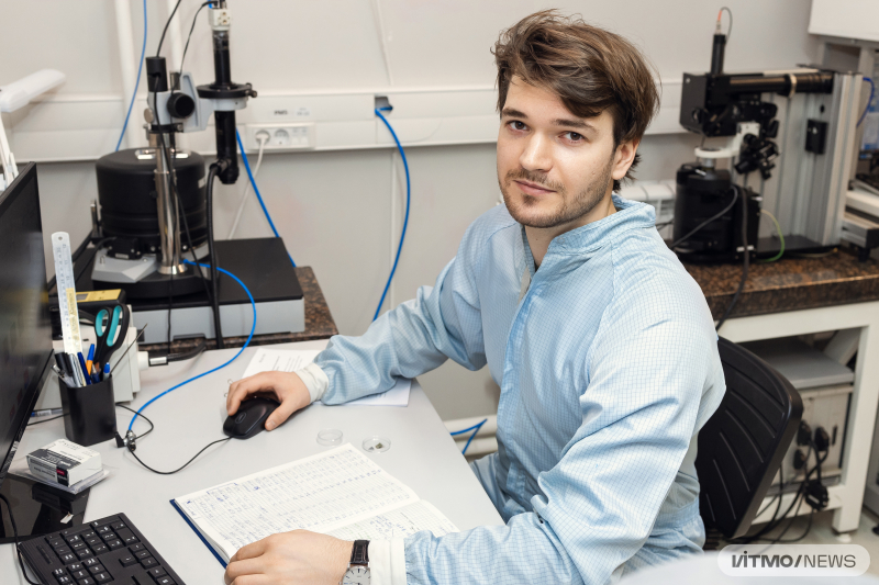
Semyon Bachinin. Photo by Dmitry Grigoryev / ITMO NEWS
The produced 2D crystals can serve as a basis for memristors – devices used to record and store information. Apart from being more energy-efficient and self-sufficient, the structures enable targeted access to specific memory cells, which isn’t possible with conventional devices. Moreover, their production doesn’t require complex lithographic technology and expensive equipment. Memristors can be used to design microoptics, as well as memory elements for computers that would accommodate more complex AI models – the crystals can function according to neuromorphic principles, imitating the function of neurons in the human brain.
This project was conducted within the Priority 2030 grant 2D Metal-Organic Frameworks: Alternative Silicon for Microelectronics supported by the Russian Science Foundation grant No. 22-72-10027 (Hybrid flexible materials as a new active layer for modern devices for data recording and storage). The study is a result of collaboration between researchers from ITMO University, Harbin Engineering University (China), King Abdullah University of Science and Technology (KAUST; Saudi Arabia), Nikolaev Institute of Inorganic Chemistry Siberian Branch of the Russian Academy of Sciences (Russia), St. Petersburg State University (Russia), and Institut Jean Lamour (Université de Lorraine, France).