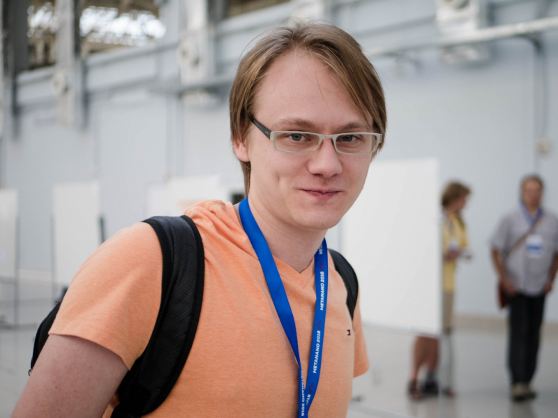
You were recently announced as one of the recipients of the Zhores Alferov Scholarship, named after the late Nobel Prize laureate. The competition received over 350 applications from PhD students and young scientists. What did you write in yours?
When you apply for this scholarship, you list all of your achievements, publications, and the conferences you’ve participated in, as well as the journals, magazines, and newspapers that have mentioned your work.
I felt like I had a chance to win, which is thanks to my research advisor Sergey Makarov as well as the entire Perolab team, with whom we’ve published many great articles in my years as a student here.
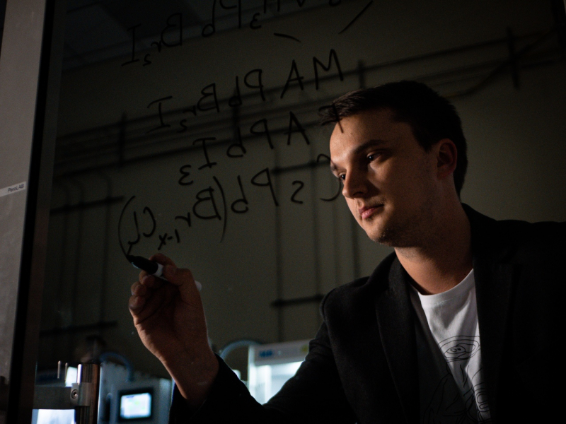
So it wasn’t a surprise to you?
It was very unexpected. Sure, I realized I had lots of articles and I had achievements, but I knew there’d be many applicants, and very few usually win. I submitted my application in June and forgot about it. Last week, I found out I won, which lifted my spirits very much – it was an unexpected pleasure. And when I found out there were only ten winners, it was almost shocking; I couldn’t believe I got into such a small winner pool.
My research advisor was the first to congratulate me, and I am very grateful to him for his patience and help. As a whole, this win isn’t mine alone: I only won thanks to the efforts of our entire lab.
If I understand it right, the Alferov Scholarship has a special meaning to you.
It does. I got my Master’s degree at the Saint Petersburg Academic University, which was founded by Zhores Alferov himself. I also got my Bachelor’s at the St. Petersburg Polytechnic University, but most of our classes were held at the Academic University, which makes it my alma mater.
Have you ever met Zhores Alferov?
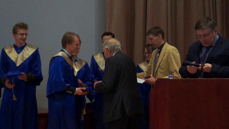
I did. When I was a Bachelor’s and Master’s student, he would give annual lectures during which he’d tell us about the achievements of Soviet and Russian science, about making heterostructure lasers, about the history of the Ioffe Institute and the Soviet nuclear program. It was interesting to find out how it all developed historically.
Perovskite nano-pancakes
What research have you been working on lately?
Most of my work nowadays concerns perovskite nanophotonics and optoelectronics. Right now, I’m studying topological effects in various perovskite nanostructures. I also have articles on the non-locality of excitons in perovskite nanoparticles (a joint study with Prof. Andrey Rogach’s team at the City University of Hong Kong) and perovskite microdisk lasers.
Can you tell us about the significance of these studies?
Regular nanostructures and waveguides always contain some kinds of defects. The result is that these photonic structures suffer from optical losses due to the scattering and refraction at corners, curves, and defects. If we create a special metamaterial – a topological insulator – we can achieve a complete lack of scattering and wave decay.
Another curious property of such structures is the presence of N-dimensional modes. By combining topological insulators with perovskites, the former possessing wonderful optical properties, we can produce highly efficient light-emitting devices, such as lasers.
Before this, I worked on the modeling of microdisk perovskite lasers, which is another very promising technology.
What are its prospects?
All processor manufacturers are currently facing a challenge: as computers reach their computational limits, it becomes increasingly more difficult to make transistors smaller and increase their effectiveness. That’s why everyone wants to move to optical computers and microchips, as it would sharply increase the speed of data transfer and processing.
To create these optical chips, we’ll need nanoscaled coherent radiation sources, among other things. They can’t be silicon-based, as that material is highly unsuitable for emitting photons. Researchers have succeeded in developing gallium arsenide-based optical devices. This material possesses great optical properties and can be used to produce solar cells, light diodes, and nanoscaled microdisk lasers. Those are “pancakes”, to put it in layperson’s terms, several micrometers in diameter and several hundreds of nanometers thick. They can’t be seen by the naked eye, as they are a hundred times thinner than a hair.
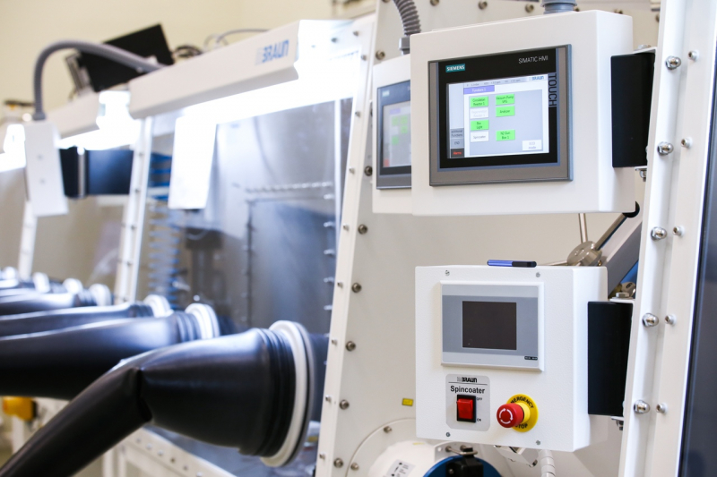
But there’s another issue – gallium arsenide nanostructures are very expensive and you need very complex and expensive equipment to make them. Everyone wants cheap ones – and that’s where halide perovskites come in. They are a relatively new class of substances that possess great optical properties just like gallium arsenide. What makes perovskites advantageous is how cheap they are to make using solution chemistry methods, as well as the tunability of their emission line.
In our research, we’ve demonstrated that perovskites can be used to create entire arrays of microdisk lasers. Potentially, these structures and topological insulators could be used to create optical microchips.
Why did you make the switch from microdisk lasers to topological states?
In research, we’re always looking for something new and interesting. Microdisk lasers are well-known and thoroughly studied, and have been around for some 20 years. Topological insulators and lasers that use them are a new concept in photonics. We thought that the wonderful qualities of perovskites would be a perfect fit for topological lasers. That’s why we’re currently working on this subject in collaboration with Alexander Khanikaev, a very talented researcher and professor at the City College of New York.
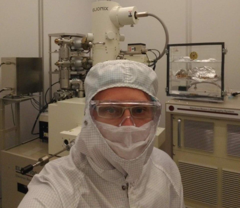
From radio club to experimental physics
How did you end up going into science?
In school, I felt drawn to physics and biology. I really liked assembling circuits and power supplies, taking things apart, soldering things – that’s where it all started. I was also into ham radio – a hobby where you use radio systems to talk to other people. It’s very interesting and unlike what you get with phones or chat rooms – you need to tune into specific frequencies and every radio operator has their own callsign. You never know who you’ll encounter every time.
I got into all these things in grades eight and nine and realized I was interested in physics. I began to pick universities in St. Petersburg to apply to – don’t know why, maybe because of my roots in the city. I’m from the Stavropol Krai, and most of my classmates either stayed down south or went to Moscow, but I was drawn to St. Petersburg, even though I’d never been there before. I ended up enrolling at the Peter the Great St. Petersburg Polytechnic University.
What was your Bachelor’s major?
In the third year, we had to choose between astrophysics, plasma physics, and nanotechnologies. I realized that astrophysics and plasma are, of course, interesting, but I like being able to touch things: microchips, structures, lasers. So I went with nanotechnologies.
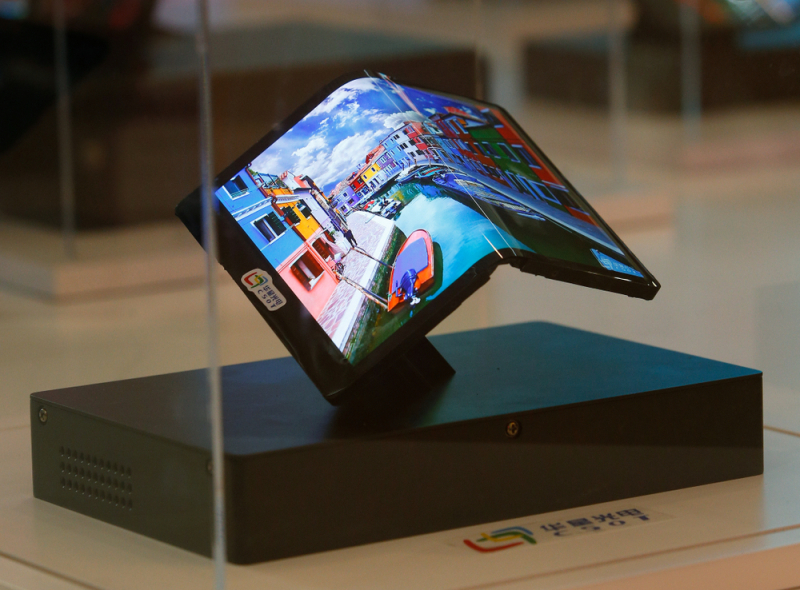
We were given tours of the labs at the Polytechnic University and the Academic University so we’d choose where to do an internship. I chose the organic electronics lab, headed by Andrey Aleshin. I enjoyed this field. It used to be that electronics only used conventional solid crystalline substances – silicon or gallium arsenide. Then, people realized that they could use polymers and create flexible structures. That’s why, for instance, flexible displays for phones and televisions are now possible. I spent three years at the lab working on flexible memory devices that were based on such polymers and graphene particles. Our devices could bend and also didn’t require external power – flexible thumb drives of sorts.
Then, I learned that ITMO won a megagrant to establish a new laboratory that would deal with perovskite nanophotonics and optoelectronics. At this point, I already knew about perovskites and their potential, so I decided to apply for a PhD program at ITMO University. It’s a memorable thing – seeing an empty lab fill up with new equipment over time.
What do you like the most about being a scientist?
Getting to study new things that people have never seen or known about. You can use your own knowledge to create impossible structures. You see topological states and how they glow. You see how beautiful it is and you know you made it yourself.
What’s a day in the life of an experimental physicist like?
At our lab, you get to choose what to do. I can start the day by calculating something, then modeling a structure, identifying the modes within it, and finding the optimal parameters. Then, others will use it to create an actual structure.
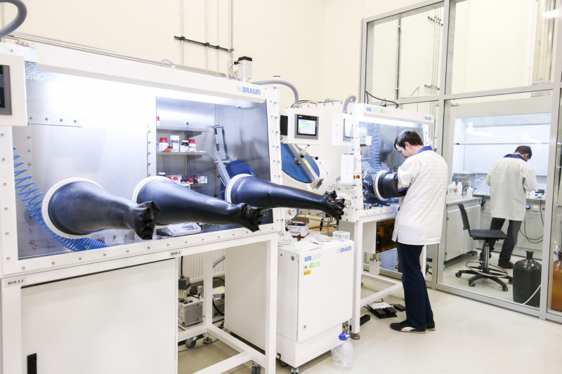
For instance, when I visited our partners in New York, we calculated and created silicon topological nanostructures. I brought them back to Russia and studied their optical qualities. The experiments are carried out in a special basement room with lots of complex equipment – lasers, spectrometers, a cryostat. And usually you’d spend hours there, in the dark.
On Italian science
From what I’ve heard, the USA wasn’t the only place you’ve worked in. What brought you to Italy?
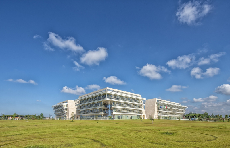
I’m enrolled in a double-degree PhD program at ITMO University and the University of Rome Tor Vergata. In Italy, my research mostly concerns the modeling of light diodes and solar cells.
What makes Italian universities different from Russian ones?
Well, for instance, our PhD programs are four years long and theirs only last for three. We spend the first two years attending lectures and seminars and taking exams: philosophy, English, and our major. In Italy, you can take all exams in the first semester. But the programs are actually similar.
What I like is that every Friday, they have group pizza lunch at the office. Everyone gets together, eats pizza, and talks lively in Italian; generally, they really love lively discussions (laughs) and having espresso.
What are your other interests besides science?
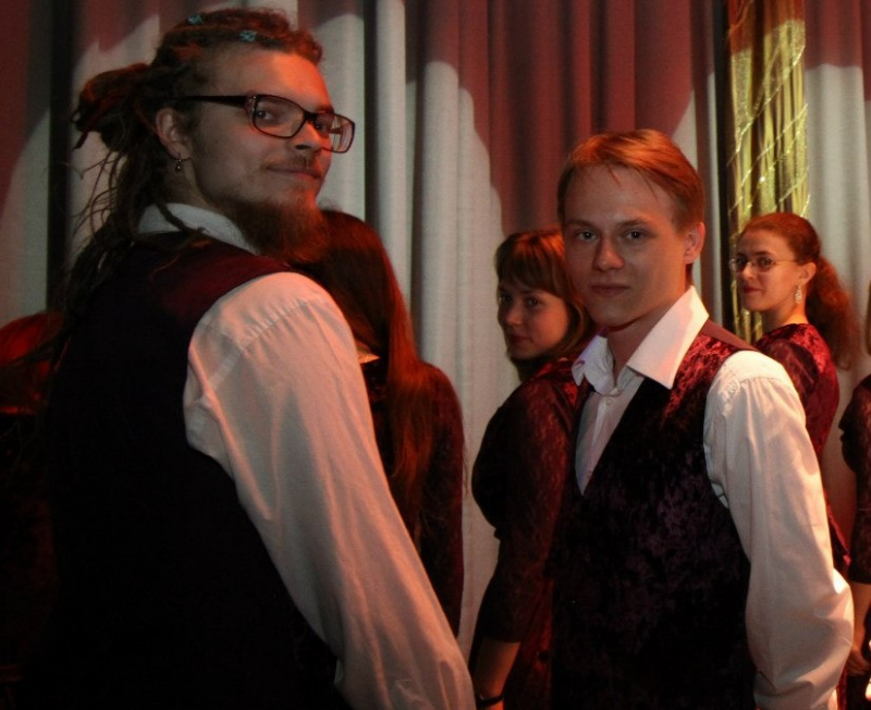
As a Bachelor’s and Master’s student, when I had more free time, I was part of the Polytechnic University’s choir. I’ve always enjoyed music, I loved singing and playing instruments. I’m very grateful to the choir – it was a welcome distraction and we even traveled. I’ve been to Germany; we did a tour of German cities: Tübingen, Stuttgart, Munich. We performed at different venues, even churches, and it was interesting to get to know their culture. That was my first time abroad. As a PhD student, I don’t have much free time, but I try to play sports, run, and cycle.
I also have a guitar that I play from time to time. Sometimes I feel like rejoining the choir and, perhaps, someday I’ll be able to.
What’s your grand ambition or goal?
As our school’s dean Pavel Belov says, one must set realistic goals, and my realistic goal, for example, is to become a professor. We’ll see where – perhaps abroad, perhaps here in Russia, at ITMO, for instance. I like our laboratory; I’ve seen many laboratories, including those in other countries, and ours is one of the best. International experience is beneficial, as you get to see how people in other countries and other teams do their work. That’s very helpful for a young scientist’s career.
