Our current smartphones and computers use electricity to transfer information, however this technology is not perfect: electronic devices waste a lot of energy as heat; moreover, their performance speed is limited. Using photons instead of electrons to encode information is a way to overcome these limitations. Photonic devices do not heat as much, consume less energy, and work faster – while maintaining the same data transfer quality.
In order to develop photonic devices, researchers create optical systems integrated on chips. These are produced with thin waveguides – layers of dielectric with a high refractive index that localize and contain light. With a semiconductor layer added to the structure, it becomes possible to generate exciton-polaritons on such chips. Exciton-polaritons are hybrid quasiparticles that have the properties of both light and matter; using them, it is possible to conduct computations using optics instead of electronics.
However, controlling and studying such particles is not an easy task because they are trapped inside a waveguide and thus do not emit light into free space. To solve this problem, physicists are developing durable photonic structures – metasurfaces that can transfer light out of the waveguide. Typically, such metasurfaces are complex and expensive to produce. Moreover, when using these structures in experiments, scientists have to rely on special microscopes – which come with their own limitations: for instance, light has to be coupled into a sample only at a specific angle, while lengthy measurements are required to visualize the interaction between light and matter.
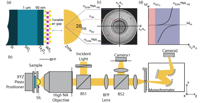
A schematic of the experiment with a solid immersion lens: a) a planar waveguide coupled with a 2D semiconductor monolayer, b) layout of the experiment, c) an image of the solid immersion lens in reciprocal space, d) a typical dispersion of an exciton-polariton. Credit: Nano Letters
A solution from ITMO
ITMO physicists have suggested their own approach to studying and controlling waveguide exciton-polaritons with a solid immersion lens. With the new method, it takes only a few milliseconds to see how light interacts with matter inside a waveguide – and control the process.
This was achieved by integrating a two-dimensional semiconductor made from a tungsten disulfide (WS2) monolayer into the waveguide and using a solid immersion lens made from zinc selenide (ZnSe) with a high refractive index. These additions allowed the researchers to visualize the exciton-polaritons inside the waveguide, as well as control the coupling between light and matter by changing the distance between the flat surface of the lens and the sample.
Moreover, controlling the strength of the light-matter interaction allowed the scientists to exclude the effect of semiconductor defects on the properties of waveguide exciton-polaritons at room temperature.
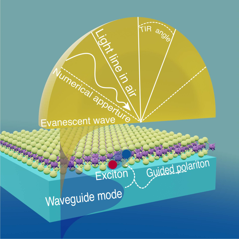
A schematic of the experiment with a solid immersion lens and a monolayer coupled to the waveguide. The researchers dry transferred the 2D semiconductor onto the sample; then they placed the sample into an optical microscope and measured it. Credit: Nano Letters
What’s next
The suggested method can be used to create a microscope capable of probing exciton-polaritons inside optical chips quickly and non-invasively. Such microscopes will be useful for creating and researching new photonic chip-based supercompact devices for optical information processing, including photonic computers.
“In this study, we have demonstrated a new physical effect, in which the use of exciton-polaritons inside a waveguide allowed us to decrease the effect of semiconductor defects on its optical properties. We have also shown how this effect can be controlled by changing the distance between a solid immersion lens and a waveguide. In the future, we are planning to use lenses with a higher refractive index, which will allow us to study structures that are smaller in volume and better confine light,” commented Valeriy Kondratyev, one of the paper’s authors, a PhD student at ITMO’s School of Physics and Engineering.
This project is supported by the Russian Science Foundation and the Priority 2030 program.
Reference: Valeriy Kondratyev, Dmitry Permyakov, Tatyana Ivanova, Ivan Iorsh, Dmitry Krizhanovskii, Maurice Skolnick, Vasily Kravtsov, Anton Samusev. Probing and Control of Guided Exciton–Polaritons in a 2D Semiconductor-Integrated Slab Waveguide (Nano Letters, 2023).