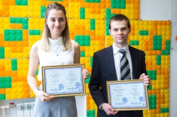
Founded in 1999, Jagadishwar Mahanty Prize is a prestigious award proffered to young scientists from all over the world for the outstanding thesis research they have accomplished when studying on a PhD at the Australian National University’s Research School of Physics and Engineering.
The candidates are selected by a special committee headed by the School’s Director. Keeping to the tradition, the award ceremony takes place on the Day of the School. According to the rules of the prize, the award can be given to several authors of equal merit at the same time, or not be awarded at all should there be no theses that managed to win the committee over. There was a clear winner this year, though: Alexey Slobozhanyuk, a research associate at ITMO University’s School of Physics and Engineering.
Topological photonics and next-generation devices: how to unite fundamental science and applied tasks
Over the course of three years, the young scientists studied at a joint ITMO University-ANU PhD program, which resulted in him getting two, Russian and international, PhD degrees. Alexey wrote his thesis, which was dedicated to metamaterials (synthetically-made new materials with unique properties) and their applications, following his extensive research work at ITMO’s International Research Center for Nanophotonics and Metamaterials, the Australian National University, and in the US at the City University of New York, where he was guided by Pavel Belov, Yuri Kivshar, and Alexander Khanikaev respectively.

“My thesis consists of two parts: the first one explored the research of new physical effects on the basis of metamaterials, while the second looked into using metamaterials for creating next-generation devices, making my work a combination of both fundamental and applied physics,” says Alexey Slobozhanyuk.
Fundamental research
In the field of fundamental research, the scientist works on topological photonics. This is a new but dynamically developing scientific area concerned with developing structures analogous to topological insulators in solid state, explains Alexey Slobozhanyuk.
What makes topological insulators so good in general? The protected state that exists at the surface of this insulating structure makes for a perfect environment to transmit electric current, shielding the electrons from external disturbances and potential defects of the material. This allows for a stable and homogenous flow of the electric current. The significance of solid-state topological insulators was recognized by the 2016 Nobel Prize in Physics, awarded to British physicists David Thouless, Duncan Haldane, and Michael Kosterlitz for their theoretical discoveries of topological phase transitions and topological phases of matter.

Together with his colleagues from an international research group, Alexey Slobozhanyuk was the first to propose a three-dimensional topological insulator for electromagnetic waves (published by Nature Photonics, this research was later named by Optics & Photonics News as one of the most promising breakthroughs in the field of optics and photonics in 2017 – Ed.). One of the advantages of this innovative material is that it can be used for adaptive manipulation of light emission, whilst also eliminating the possible losses caused by absorption and dispersion on defective areas.
“We also look at these structures from the electromagnetic viewpoint, swapping electrons for photons. The main objective here is to create new kinds of flexible waveguides. Currently, if you take existing optical fibers and bend them, there will be light dispersion at the plication, or defective, area. But if the optical fibers are made from our proposed material, then the light will disperse evenly without any reflection or reverse dispersion in spite of the defects. That’s why you could say that what we work on are next-generation, super-effective structures,” comments the researcher.
Topologically protected transfer of signals will be a major step forward to the improvement of communications lines, antennae and optical computers. Metamaterials-based topological insulators will allow for complex manipulations of light at the scale significantly smaller than the wavelength, which is practically impossible to carry out with available technologies. This is important for the new optical chips and technologies of the future, given the dominant trend of the miniaturization of devices, adds Alexey Slobozhanyuk.

Innovative devices
The second part of the scientist’s award-winning thesis was dedicated to applied research: working with Dutch and Australian scientists as part of an international research initiative, Alexey Slobozhanyuk found a way to increase the resolution capacity of MRI scanners, whilst also making the procedure faster and safer for patients.
What the group posited in particular was that the issue of low image resolution could be solved by adding a special metamaterial-made base layer. Placing this layer inside an MRI scanner makes it possible to increase the signal-to-noise ratio in the scanned area, which leads to a significant rise in resolution capacity of the device and a no less significant acceleration of the scanning speed.
“In a conventional MRI approach, when you examine, say, a patient’s brain, you have to make them put on a special helmet. This is in fact a radiofrequency coil which acts as a signal receiving device, and it is its sensitivity that the quality of the image you receive ultimately depends upon. Because of the signal-to-noise ratio in MRI being so little, patients have to spend as much as 20 to 30 minutes lying inside the MRI scanner. It’s a far cry from X-ray fluorography where you get the image almost immediately. Due to the low sensitivity of MRI coils, one procedure is usually repeated several times to store up the signal, and this takes time,” shares Alexey. “What we did was to create a new passive device, a special base layer, which is inserted between the coil and patient. This layer increases the receptibility of the coil by upping the signal-to-noise ratio, or, in other words, by redistributing electromagnetic fields to extremely small distances which are a lot smaller than the wavelength. This intensifies the local magnetic field, leading to an increase in the signal-to-noise ratio.”

What makes the metamaterials-made coils so important is that by improving the resolution of the MRI images, they allow for an earlier diagnosis of diseases. In addition to their effectiveness, these devices are also safe for patients to use.
“People with metallic implants can’t undergo procedures on the 3 Tesla MRI scanners because being exposed to electromagnetic radiation makes these implants heat up. The structure we invented allows for a significant decrease in the radiofrequency pressure experienced by patients. It also makes for the procedure being more adaptive: by using our coil, you can highlight the exact area you want to transmit the signal, so that if you want to create an image of a patient’s limb, you no longer have to irradiate their whole body. Our structure focuses the electromagnetic field in the highlighted area, minimizing its intensity in other areas of the body,” adds the researcher.
The innovative radiofrequency coils have passed clinical trials in the Almazov Center in St. Petersburg and are already being used in the Center’s day-to-day medical practice, says Alexey Slobozhanyuk.

Prospects of the research
As of now, the scientist carries out applied research and commercialization of innovative devices developed in the International Research Center for Nanophotonics and Metamaterials. He also continues his close cooperation with international partners, namely with Prof. Alexander Khanikaev from the City University of New York, and works with the world-class research institutions in Australia, the US, the Netherlands, France and Finland.
“I’m interested in creating something that would enter our day-to-day in the nearest future, not somewhere along the line in 20-30 years. For example, our MRI coils are already applied in the Almazov Center. We’re also using these innovative materials to develop other next-generation solutions for a wide range of other fields,” comments Alexey Slobozhanyuk.
The research group Alexey works in also sees it important to interact with industrial partners to identify the inventions that would meet their needs and demands.

“Knowing the problems we could solve by creating new technologies means we can launch these on the market much faster than we would otherwise. That’s why in my work, I try to connect these two communities, scientists and industrialists, together, with the aim of developing innovative and effective devices in Russia,” says Alexey. “Australia and the US, which are other countries I’ve lived in, both have a very strong and well-functioning connection between science and the industry. They create non-governmental funds for supporting promising scientific initiatives. Their philanthropists and people of business invest huge amounts of money into specific research groups as a way of supporting innovation-oriented projects, getting a share in intellectual property rights in return. This is the model I try to promote here in Russia. I’m convinced that with a better interaction between entrepreneurs and science, we’ll arrive at a new stage of technological progress much faster.”


