Nowadays, devices that are based on microscopic lasers and optical chips are becoming more and more common. They are used in the production of lidars, in the development of new biosensors, and in the future, they can become the foundation for new optical computers that will use photons rather than electrons to transfer and process information.
Most of today’s optical chips operate in the infrared (IR) band, i.e. the lasers they use emit in the IR range that is invisible to the human eye.
“But to make the devices even more compact, we need to work in the visible range,” says Sergey Makarov, chief researcher at ITMO’s Department of Physics and Engineering, “as the size of a chip depends on the wavelength of the emission of its light source.”

Silicon issue
An optical chip consists of such components as lasers and waveguides. While creating a source that would emit in the green or red spectra is quite easy, a proper waveguide for this spectral range can be an issue.
“A microlaser is a source of emission that you need to guide somewhere,” comments Ivan Sinev, senior researcher at ITMO’s Department of Physics and Engineering, “and this is what waveguides are for. But the standard silicon waveguides that are used in IR optics don’t work in the visible range. There, they transmit signal no further than several micrometers. For an optical chip, we need to transmit on tens of micrometers with a high localization, so that the waveguide would have a very small diameter and the light would travel sufficiently far through it.”
Earlier, attempts were made to replace silicon waveguides with silver ones, but the transmission distance in such systems was also insufficient.
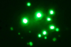
Optical chip in a Petri dish
In the end, a team of scientists that included specialists from ITMO University, St. Petersburg Academic University, and Université de Lorraine decided to use gallium phosphide (GaP). This material has very small losses in the visible range as well as high refractive index. The microlaser itself was made of halide perovskite. But the most important thing is that the laser was grown directly on the waveguide in a common Petri dish.
“The beauty of this approach is that we create perovskite microlasers with nano-waveguides embedded in them right from the start,” notes Sergey Makarov, “which is done by co-crystallizing GaP of the waveguide and the perovskite microlaser in a solution of perovskite ink. This means that rather than using expensive nanolithography methods, we use those of solution chemistry, which are a lot cheaper and easier. After that, the laser and the waveguide are planted on a substrate, thus forming the base for the optical chip.”
The resulting systems can transmit signals for a much greater distance than their counterparts with silicon or silver nano-waveguides. At the same time, the size of these chips is about three times less than that of its IR band analogues.
Color adjustment
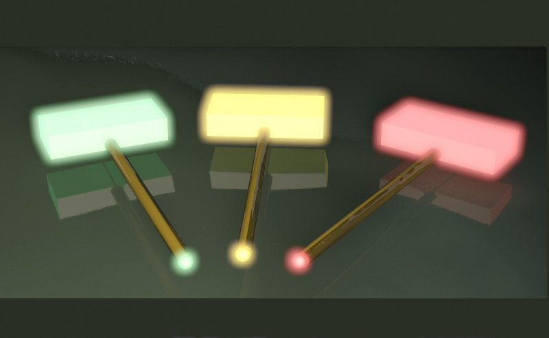
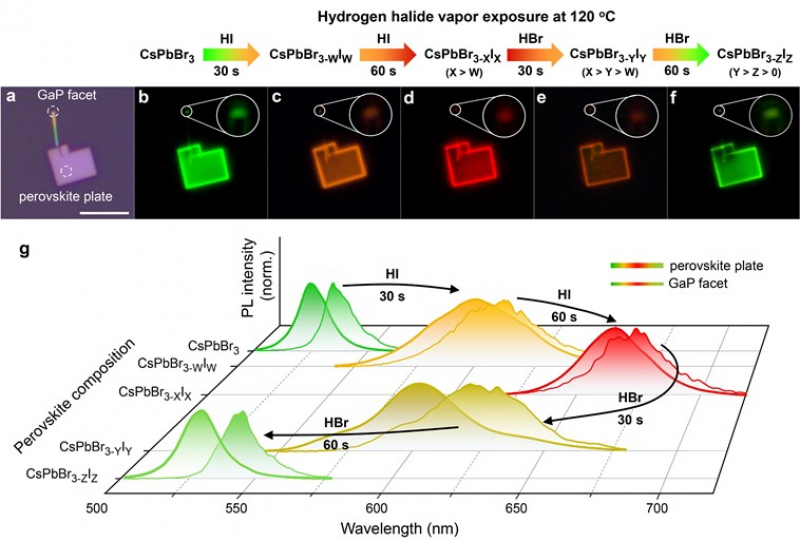
Another important feature of the chip is the ability to adjust the emission range of a laser from green to red spectral range. Moreover, you can change the emission color after the chip production, and this process is reversible.
“This change is done via a chemistry method,” explains Anatoly Pushkarev, senior researcher at ITMO’s Department of Physics and Engineering. “We put the substrate with an optical chip into the vapors of hydriodic or hydrobromic acid for just a couple of minutes. This is quite enough time for the anionic exchange between the perovskite microlaser and the acid’s molecules to take place, which changes the chemical composition of the perovskite, and therefore the wavelength of its emission.”
This can be useful for the devices that have to transmit many optical signals at different wavelengths. For example, you can create several lasers for such a device, connect them to a single waveguide, and use it for transmitting several signals at different wavelengths at once.
Antenna
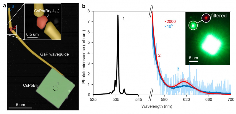
The scientists also equipped the newly created chip with an optical nanoantenna made of perovskite that receives the signal travelling along the waveguide and allows uniting two chips in a single system.
“We added a nanoantenna at the other end of our waveguide,” explains Pavel Trofimov, PhD student at ITMO’s Department of Physics and Engineering, “so we have a light source, a waveguide and a nanoantenna that emits light when pumped by the microlaser’s emission. Then we attached another waveguide to it: as a result, the emission from a single laser went into two waveguides. At the same time, the nanoantenna did not just unite the two waveguides into a single system, but also transformed part of the green light into the red spectrum. So we had one wavelength - and got two, a single channel - and then two of them.”
The research was published in ACS Nano, one of the leading scientific journals.
Reference: Pavel Trofimov, Anatoly P. Pushkarev, Ivan S. Sinev, Vladimir V. Fedorov, Stéphanie Bruyère, Alexey Bolshakov, Ivan S. Mukhin, and Sergey V. Makarov. Perovskite - Gallium Phosphide Platform for Reconfigurable Visible-Light Nanophotonic Chip, ACS Nano, 2020/10.1021/acsnano.0c01104