Promises of 2D materials
According to Moore’s law, the number of transistors that can fit into a processor doubles every year – and, excluding some small deviations, this has been true for over fifty years. However, some researchers posit that there will be a time when this number simply won’t be able to double: by 2060, the chips would have to be the size of an atom to get any smaller, which is ruled impossible by quantum mechanics.
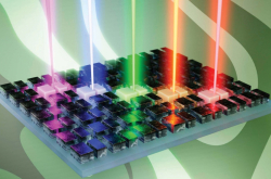
Nevertheless, latest discoveries demonstrate that one atom is the minimum possible thickness of low-dimensional materials. Graphene and silicon, traditionally used in electronics, won’t be suitable for such materials – and that’s where 2D materials from photonics and optoelectronics come into play. For instance, dichalcogenides of transition metals have already been used to design lasers, optical switching devices, and one-atom-thick nonlinear optical elements.
Moreover, dichalcogenides in 2D materials are rather pliable, which enables their application in flexible electronics: they can be built into clothes as personal electronic devices or implanted under human skin as medical sensors.
“The first monolayer from a dichalcogenide of a transition metal was synthesized in 2013-2014. In 3D, it is just a black graphite-like substance that doesn’t pose a lot of interest for opticians; however, a one-atom-thick layer of it will turn into an optically active semiconductor. Ever since their discovery, such materials have been actively studied and some researchers predict that they will prove useful in practical applications of optoelectronics,” explains Ivan Iorsh, a chief research associate at ITMO’s Faculty of Physics.

Ivan Iorsh. Photo by ITMO.NEWS
Challenges in application
2D materials have the thickness of a single atom and are similar to graphene, but have a different composition and geometry, as well as demonstrate semiconductor properties. Moreover, they interact with light, which means they can be used to develop electronic devices such as lasers. However, such applications are not easy to implement because their extreme thinness leads to strong Coulomb interactions, which means that electric charges within the material are strongly attracted to one another. That’s why optical responses of such materials are defined by excitons – bound states of electrons and electron holes. These states are similar to hydrogen atoms, but instead of the nucleus there is a positively charged hole with an electron orbiting it.
According to one classification, there are dark and bright excitons. Contrary to the latter, dark excitons have nearly no interactions with light, which renders them useless in the production of optical devices.
“Different exciton states have different energy, lower in some and higher in others. If we resonantly pump systems of such bound electron-hole states, they interact with the material’s crystalline grid and most of them aim to get to the lowest energy state. It turned out that if a dark exciton has this lowest energy state, it will poorly interact with light, despite the fact that it’s a direct-gap semiconductor, especially in lower temperatures. If the temperature is high, the exciton can transition from the dark state to a higher energy level and start radiating. However, if the material is cooled down, the exciton will turn dark again. This property can be beneficial in some applications, but it won’t be if we are trying to produce lasers or diodes,” says Ivan Iorsh.
This brightening of dark excitons in low temperatures is one of the crucial tasks of photonics and optoelectronics. One solution is to subject the material to a strong magnetic field; however, it is neither affordable nor practical, because a power-intensive superconducting magnet the size of a room would be needed to produce a small laser.
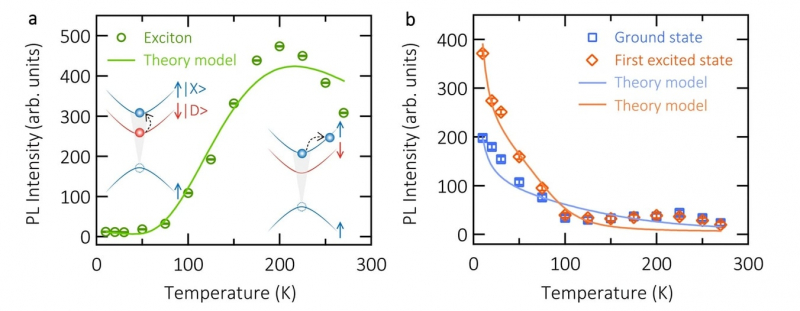
Integral temperature dependencies of fluorescence in regular excitons (a) and exciton-polaritons (b). As seen on the plot, regular excitons stop radiating in lower temperatures, while a reverse dependence is seen for exciton-polaritons. Images from the article, credit: nature.com
Solutions by ITMO researchers
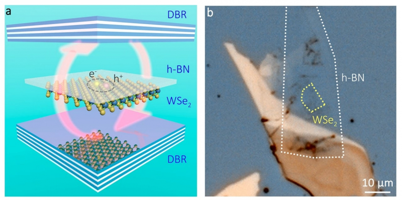
Three years ago, physicists from ITMO University came up with another possible solution. They suggested using a system in which the lowest energy state corresponds to a dark exciton and the highest – to a bright one, and putting inside a resonator consisting of two mirrors in parallel to each other. This would result in the bright exciton coupling with a photon and then splitting into two polaritons with different energy content. One of the polaritons will be on a lower energetic level than the dark exciton – and this would mean that it will turn into a bright one. In this case, the 2D material inside the resonator will radiate light in low temperatures.
This year, the researchers and their collaborators from Germany proved this theory using wolfram selenide (WSe2). In their experiments, they have plotted photoluminescence as a function of temperature for a 2D material placed inside a resonator. This function turned out to be reverse to that of classical 2D materials based on dichalcogenides of transition metals: the higher the temperature in the resonator, the lower the efficiency of photoluminescence.
Other promising studies of 2D materials
Quantum communications are the new promising field – they are studied at ITMO and major companies, and they are used on the ISS. However, a more efficient photon source is necessary for efficient quantum communications. The authors of the article believe that 2D materials based on dichalcogenides of transition metals are promising candidates for this position, because even now there are methods for their controlled production.
Another area of application for this novel group of 2D materials is based on the magnetic properties of some of its members. The goal is to discover whether these properties can be controlled optically. If such mechanisms were to be discovered, these materials can be used in developing magnetic random-access memory.
Reference: Hangyong Shan, Ivan Iorsh, Bo Han, Christoph Rupprecht, et al., Brightening of a dark monolayer semiconductor via strong light-matter coupling in a cavity (Nature Communications, 2022).