Mikhail Omelyanovich presented an application of laser ablation to solar panels using perovskites at the Contest for Technological Projects organized by Rosnano Fund for Infrastructure and Educational Programs and took first place. The developer was awarded with visiting the largest European technological center in Belgium.
What are disadvantages of solar panels?
First of all, the efficiency of solar panels is only 20-25%, but at the same time they are very expensive due to silicon which has to be developed in a laboratory. As of now, scientists work on a new type of panels based on perovskites instead of silicon, as it can absorb solar energy more effectively. Furthermore, the elements made of this material are cheaper and their development is easier. One can cover any surface with perovskites – and the layer will be thinner than one made of silicon. For instance, a silicon layer size of 180 micron absorbs the same amount of light as a perovskite size of 1 micron. The researchers of a new lab at ITMO are going to study this promising material.

Solar panels credit:depositphotos.com
To develop conductive contacts for perovskite solar panels one uses pulsed laser deposition or laser ablation. It is a method of mass transportation from a surface with a laser pulse.
Usually one equips solar panels with contact elements and perovskites using different equipment, as these are different processes. Mikhail Omelyanovich offered to develop a new type of equipment which would be able to combine these processes as fixing perovskites and contact elements. According to the researcher, it was an obvious idea, but nobody turned it into reality.
As of now, upper contacts are fixed right above a panel, so they partially shade an absorbing matter – this reduces the efficiency of the photocell. Mikhail offers to put conductive contacts under the perovskite layer. It will ease the repairmen process as one can “erase” a semi conductive layer and other elements with new ones without disturbing the elements that work properly.

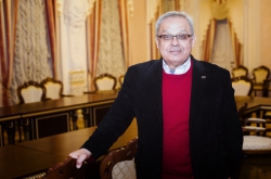
Mikhail Omelyanovich
“We don’t aim to make 100% effective and long-lasting panels – we want to invent a panel which can be fixed easily without spending lots of money. We also strive to make them more eco-friendly by replacing lead with something else. Theoretically one can use a matter which one can remove from conductive contacts and then vaporize. Despite that fact that such technologies already exist there is one engineering challenge. How to apply these solutions to develop a cheap and at the same time effective panel? What materials should be used to make a panel relevant for mass production?” commented Mikhail Omelyanovich.
Mr. Omelyanovich tries to develop a perovskite solar panel that would be interesting for investors. As of now, he conducts experiments in order to find a proper technology for developing a perovskite photocell with a backside contact.
Mikhail’s project was placed 1st at the all Russia engineering contest initiated by Rusnano. One of the main requirements was to present a project that would have potential for commercialization. The organizers of the contest chose the best tech solutions to apply them to a new nanocenter Tekhnospark.

Winners of the Rusnano engineering contest credit:rusnano.com
The winners came to Belgium to visit the largest European innovation hub at the University of Leuven and learned how Europeans develop hi-tech companies. They also visited its nanocenter, faculties of biotechnologies, chemistry, composite materials and additional technologies.
“The main perk of KU Leuven is that its chemists, biologists and specialists on nanotechnologies work nearby each other. It gives an opportunity to exchange knowledge and ideas when conducting experiments – this helps make great discoveries,” added Mr. Omelyanovich. Mikhail also believes that ITMO has all the necessary facilities to create the same hi-tech cluster.