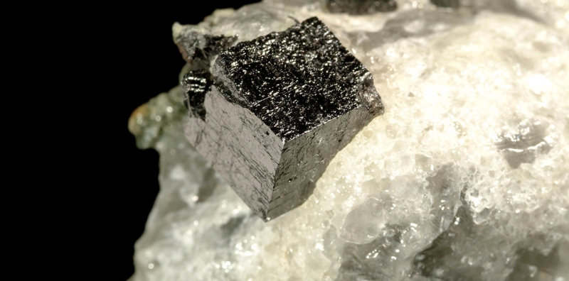
Halide perovskite is a relatively new material in nanophotonics, and was first used in solar cells around a decade ago. In its structure, this artificial material is identical to natural perovskite, discovered in the Ural Mountains in the 19th century and named after Lev Perovski, a Russian Home Affairs Minister and an avid mineral collector.
Despite the fact that many scientists around the world have been trying to apply halide perovskite in the production of industrial solar cells for years, many qualities of this metamaterial remain debatable and mostly unclear to the academia. That is exactly why a group of researchers from ITMO University decided to summarize all the information on perovskites available in an article for Applied Physics Reviews. The effort was marked by appraisal by the journal with its editor-in-chief personally calling the article one of the issue’s best.
“It was important for us to show the advantages this material has over those previously used in meta-optical and nanophotonics elements,” says Sergei Makarov, one of the authors of the paper. “We hope that our article creates an interest in developing new opto-electronic devices using perovskites across the optics community. It will open up many possibilities in the field. I assume that the editorial board appreciated our interdisciplinary approach and the fact that we tried to make additional calculations to unite all of the previously separately published data under one idea.”
An adaptable metamaterial
One of the key advantages of perovskites is their adaptability: depending on the task at hand, a perovskite-based metamaterial can be easily reconfigured by using different chemical elements to create it.
“There is such a term as a band gap in semiconductors. It’s an energy range in which an electron cannot exist in a given material. This band gap is fixed in conventional semiconductors, like silicon or gallium arsenide, whereas in perovskites we can change it by halide substitution. In layman’s terms, it means substituting one of the material’s components, namely the halide anion, with another chemical element of the same group. For example, we can replace a bromine atom with iodine or chlorine and vice versa. Moreover, this process is reversible and the qualities of the material can be restored in their place if needed. Thus, by variating the band gap we can adjust the material to functioning in different wavelength ranges. For instance, we can create an LED that is blue, green or red. The same goes for solar cells - they can absorb only a part of light, only in a specific range and we can move this range depending on the issue at hand,” explains Pavel Voroshilov, co-author of the paper.
This adaptability of perovskites makes them suitable for use in space-effective radiation sources. Furthermore, they can be changed in situ, after they have already been created, which means new opportunities for perovskite-based devices.
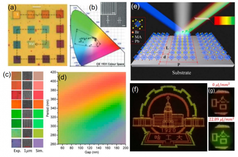
“Everyone is interested in creating miniature light sources. With perovskites we can not only set the initial qualities of the material, but also relatively easily change them on the go. This allows us, for example, to switch between different colors for one and the same LED. In a nutshell, it allows us to create color pixels consisting of only one such adaptable LED instead of three from the standard RGB-scheme, which means we can minimize the physical scale of the pixel itself. It is important because some qualities of the perovskites can make them a prospective material for a new generation of LED screens,” adds Voroshilov.
Beating silicon
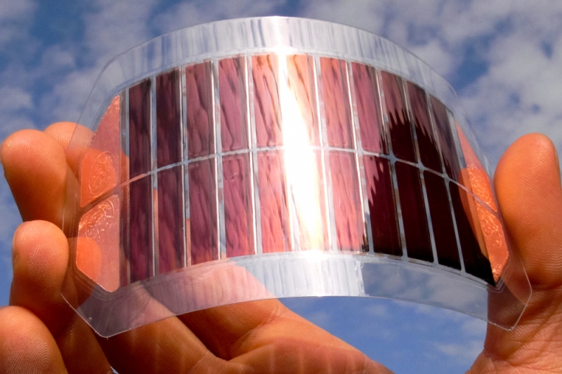
One other advantage of halide perovskites over gallium arsenide or silicon is that the costs of producing nanostructures based on them are relatively low. Production methods based on conventional semiconductors usually require expensive processing units and costly synthesis methods.
“Perovskite production is easier because their chemical production methods are accessible and compatible with roll-to-roll processing. The latter allows us to spread nanomaterials on the substrate beneath it. These nanostructures can have different forms: we can create nanospheres, nanocubes, microdiscs and there are even ways to create perovskite-based nanowires. For example, cubical perovskite nanoparticles can be obtained by chemical vapor deposition or ligand precipitation. It is possible to produce silicon nanostructures of this form, but it is trickier and more expensive. If we need periodic structures, perovskite allows us to simply use nanoprinting. We can make a template and then imprint it on the substrate to shape it into the form we need,” clarifies Voroshilov.

Yet perovskites still have not taken their rightful place in the LED and solar elements market. Experiments and theoretical findings run by Voroshilov, Makarov and coauthors can speed up the process.
“Apart from the review section, our paper includes an original study of optical resonance that can occur in perovskite-based nanostructures. We have discovered a broadband Kerker effect, previously observable in other materials but not considered in perovskites. It allows us to create directed light diffusion. Basically, we have a perovskite nanocube and irradiate it with a flat wave, but it does not diffuse anything back, meaning that it gives no reflection,” he continues.
This effect can be effectively used in various areas of nanophotonics to produce nanolasers or more efficient LEDs. The benefits seem most noticeable when we consider solar cells.
“Based on this effect, we can make an anti-reflective coating. It helps with reducing reflection from a surface. Normally, when light hits a solar cell a part of it is reflected because of the contrast between the air and the structure itself. It is a loss, as the reflected light could have been absorbed. An anti-reflective coating on the surface of solar cells makes the light pass through to the active layer loss-free, improving the device’s efficiency”, concludes Voroshilov.
According to one of the most renowned authors of the paper, Yuri Kivshar, in the future, perovskites can beat silicone and become the most convenient material for nanophotonic devices.
“Halide perovskites can be used as resonant materials with a high gain coefficient, which makes it possible to create nanolasers scaled less than 420 nm. Recent inventions can have a strong impact on designing cutting-edge optoelectronic devices with optimised optical qualities,” shares Prof.Kivshar.
Translated by Catherine Zavodova