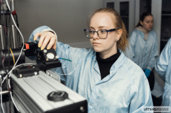
Interest in the creation of new devices and tools based on the use of semiconductor nanocrystals has grown greatly in recent years. This technology is seeing a great deal of use in biology, medicine, optical materials, electronics, solar energy and other areas. The reason for this steadfast adoption of semiconductor nanocrystals are their unique properties. Today, by changing the chemical composition and morphology, scientists can easily modify the optical response of semiconductor nanocrystals.
Another powerful tool that may be used to change the nanocrystals’ optical response is lattice distortion. In their research, the scientific team from ITMO University’s Modeling and Nanostructures Laboratory, led by Ivan Rukhlenko, has proposed a theoretical description of a new method of studying the optical properties of semiconductor nanocrystals with crystal lattice defects. The authors have considered nanostructures of various shapes and developed general methods for calculating their linear and non-linear optical properties.
“The fundamental significance of our research lies in that it offers a new method of constructing semiconductor nanoobjects. It is known that nanoobjects can be used both as stand-alone quantum structures and as elements in the creation of more complex quantum superstructures. In our study, we model the properties of a single nanoblock. We do that on two levels simultaneously - the crystal lattice and the crystal form. By choosing a form and adding defects and deformations of the nanoblock’s crystal lattice, we can significantly change its properties and amplify the desired effects. This approach, in particular, lets us turn nanoblocks that were not previously optically active into such. Structuring these nanoblocks will later facilitate the creation of next-generation optical devices,” - comments Anvar Baitmuratov, author of the article published in Nano Letters and researcher at the laboratory.
Using the developed geometrical transformation, one can, in a virtual space, “unfold” a nanoroll into a nanoplate in a curved space and calculate its optical properties.
The developed theoretical approach has found further development in another study, one focused on semiconductor nanorolls. A nanoroll is a nanoplate that, due to a particular mechanical impact, has taken the form of a multi-layered tube. What makes these objects unique is their structure: unlike nanoplates, nanorolls take up relatively little space while also preserving the bigger part of the area of nanoplates. All this allows them to interact with other nanoobjects, including molecules, with high efficiency.
In an article published in ACS Nano, a group of researchers from ITMO University have developed a new method of geometric transformation that makes it possible to “unfold” a nanoroll into a nanoplate and, therefore, calculate the optical properties of a nanoplate in a curved space.
“This method is analogous to the one that is used, for example, in Einstein’s general theory of relativity. Using this transformation, we have been able to calculate the optical properties of such a nanoplate in a curved space and recording the nanoroll’s optical response,” - says Nikita Teplyakov, author of the article published in ACS Nano and researcher at the laboratory. - “As of now, such objects are studied only experimentally. The scientific community right now is concerned more with the chemical characterization of nanorolls’ properties or the development of new methods for their production, but not with the theoretical description of the finished nanorolls’ properties. Our research is making up for that imbalance”
Thanks to their large contact area, nanorolls are used in medicine and chemistry - as catalyzers in chemical reactions, tools for capturing and transferring molecules, in molecular sensing and to determine the molecular composition of an environment. In addition, since nanorolls are chiral objects, another promising application for such objects is in spintronics, which, unlike traditional electronics, implies energy and data transfer not through electrical charges, but through their currents’ spin. Nanorolls also let us study the spin transfer in chiral molecules, notes Nikita Teplyakov.
In future, researchers plan to develop this theoretical approach for studying the optical properties of semiconductor nanocrystals with lattice defects in working with nanorolls of much bigger size, as well as other objects - nanorods and nanoplates of various shapes.
Reference: A. S. Baimuratov, T. P. Pereziabova, W. Zhu, M. Yu. Leonov, A. V. Baranov, A. V. Fedorov, and I. D. Rukhlenko, Optical Anisotropy of Topologically Distorted Semiconductor Nanocrystals, Nano Lett., Article ASAP, DOI: 10.1021/acs.nanolett.7b02203 (2017).
Reference:: N. V. Tepliakov, A. S. Baimuratov, I. A. Vovk, M. Yu. Leonov, A. V. Baranov, A. V. Fedorov, and I. D. Rukhlenko, Chiral Optical Properties of Tapered Semiconductor Nanoscrolls, ACS Nano, 11 (7), 7508–7515 (2017).