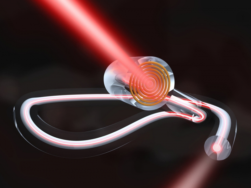
Optical fibers are widely used in the field of telecommunications, allowing the optical signal to transfer almost a million times more data than an electric signal does via a copper cable. What’s more, optical fibers are used in everyday medicine, for example, for the in vivo (within living organisms or cells) studies. For instance, endoscopy methods employing optical fibers make it possible to examine people’s internal organs in real time, which is extremely essential for diagnostics purposes.
However, the efficiency of light in-coupling by optical fibers rapidly decreases at large incidence angles. It happens so fast that at the incidence angle of 15 degrees, the efficiency drops almost to zero. This deficiency significantly limits the functional capabilities and the potential of optical fibers application.
In collaboration with the Leibniz Institute of Photonic Technology (Germany) and Australian National University, ITMO scientists Oleh Yermakov and Andrey Bogdanov resolved the fundamental problem of light coupling into optical fiber at incidence angles of over 70 degrees.
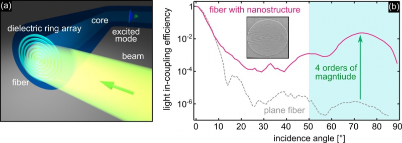
The researchers used a dielectric nanostructure with a high refractive index, made of silicon nitride, implemented at the end face of the optical fiber. More light goes to the fiber due to the low absorption losses of silicon nitride. Besides, the nanostructure is a ring-like diffraction grating. Thanks to diffraction, light passes the structure in such a way that it propagates exactly along the optical fiber axis even under a large incidence angle. Finally, the structure's ring-like shape makes it possible to capture light of any polarization and incident from any direction, which is of great importance from a practical standpoint. All these factors contribute to increasing the light in-coupling efficiency by 4 orders in comparison with optical fibers without nanostructure or with a metal nanostructure.

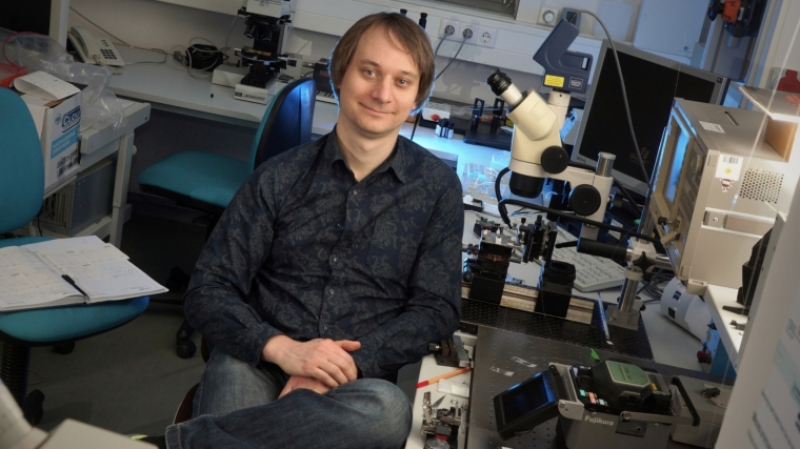
“I think we succeeded due to the harmonic combination of specialists in the fields of optical fibers and optical nanostructures, and teamwork between theoreticians and experimenters,” explains Oleh Yermakov, a graduate of a PhD program at the Department of Physics and Engineering of ITMO University. “We advanced from a superficial understanding of the problem to a detailed concept, analytical description, and a precise numerical model. This helped us come up with the optimal structure design which was then fabricated and measured by our German colleagues.”
In the nearest future, the researchers plan to speed up, simplify and cheapen the process of nanostructures fabrication by using nanoimprint lithography, assuming the polymer resist stamping and the consequent etching. For now, scientists transform their theoretical advances into an automatic algorithm based on advanced optimizers and machine learning in order to find a nanostructure design for any particular task.
“The implemented device is useful for any application that demands to remotely collect light under a large angle, as for instance in in-vivo spectroscopy or quantum technology,” comments Markus Schmidt, Professor for Fiber Photonics at Leibniz-IPHT and the head of the project.

“For many years a success of nanophotonics developed for an efficient control of light-matter interaction was not connected with the progress in fiber technologies aiming to operate on much larger scales. This work provides a bridge between two fields, and this fact was acknowledged by highlighting the paper on a front cover of ACS Photonics with the impact-factor 7.3,” says Yuri Kivshar, an Honorary Professor of ITMO University and a fellow of the Australian Academy of Science.
The research was conducted with the support from the Foundation for the Advancement of Theoretical Physics and Mathematics “BASIS”, the German-Russian Interdisciplinary Science Center (G-RISC), and the Russian Science Foundation.
Reference: Oleh Yermakov, Henrik Schneidewind, Uwe Hübner, Torsten Wieduwilt, Matthias Zeisberger, Andrey Bogdanov, Yuri Kivshar, and Markus A. Schmidt. ACS Photonics. doi.org/10.1021/acsphotonics.0c01078
