Metal-organic frameworks 101
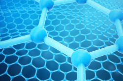
Metal-organic frameworks (MOFs) are a special class of hybrid materials. These are microporous structures with pores that are just nanometers in size. The lattices of MOFs are made with ions of metals that are connected by organic ligands.
By changing the ions and ligands that make up an MOF, it is possible to produce structures fit for various applications, such as gas catalysis, adsorption, and storage. For instance, a promising application of MOFs is as gas sensors; these devices are used in production and at labs to detect leakages of harmful gasses.
MOFs can be manufactured to have a high optical feedback – and such structures are what scientists at ITMO focus on. According to Pavel Alekseevskiy, a junior researcher at the Faculty of Physics, a certain ligand can enable a 2D MOF structure to efficiently absorb ultraviolet radiation. For a zinc-based MOF, the benefits are the simplicity of its synthesis and the wide availability of this metal. Its 2D structure also provides the material with thermostability: the heat it receives from radiation spreads evenly through the framework. These properties play a role in the creation of optical sensors and make it possible to measure optical feedback.
Carving out a unique approach to 2D MOFs
Pavel Alekseevskiy admits that advancing from lab- to mass-produced MOF-based sensors is not an easy feat.
First of all, these sensors have to be rather compact, which means that they have to be made from thinner materials. The currently synthesized MOFs are over 100 nanometers thick – and only materials that are several nanometers-thick can be used in more miniature sensors.
Secondly, in order to enable MOF-based sensors to absorb more substances from their environment and thus react to subtle changes, the surface of an MOF has to be as big as possible. This condition is nearly impossible to fulfill now because there is no single “recipe” for producing frameworks with such a length-to-thickness ratio. Each new MOF requires a separate approach.
A possible solution is to switch from using a 100 micrometer-high crystal to using layers of this same crystal that would be mere nanometers in height.
“Earlier, the efforts of scientists focused on obtaining many layers that are several nanometers in height and under 1 micrometer long. These parameters won’t work for optical devices such as sensors. They require thin and long layers, which is a new and unsolved task,” says Anastasiia Efimova, an engineer at the Faculty of Physics.
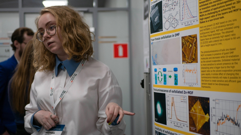
Anastasiia Efimova presenting the project at a conference. Photo courtesy of the subject
In order to obtain such layers of 2D MOFs, the researchers use exfoliation – the process can be compared to taking pages out of a book.
“Imagine that a multilayer 2D MOF is a closed book, while its layers are pages. Your task is to somehow take one page out of the book. You can’t just rip a piece of it because the bonds in the plane of the page are quite strong. However, the interlayer bonds on the surface of each page that connect the pages together are weak. That’s why you can extract the pages one by one, starting with the ones on the top. It’s important to keep them intact, without damage or tearing, during the process,” explains Pavel Alekseevskiy.

Pavel Alekseevskiy. Photo by Dmitry Grigoryev / ITMO.NEWS
However, even tried-and-tested methods are no guarantee for acquiring intact layers. According to Anastasiia Efimova, the difficulty in exfoliating 2D MOFs is in the abundance of their variations. Each of them requires an optimal exfoliation method with its own optimal parameters.
The new suggestions
Researchers from ITMO, Tianjin University (China), University of Lorraine (France), and the Nikolaev Institute of Inorganic Chemistry of the Siberian Branch of the RAS have conducted a series of experiments and compared three popular methods for exfoliating 2D MOFs based on zinc and the ligand H4TBAPy.
Each of the three methods has a different effect on the MOF. In the first experiment, 2D MOFs were subjected to ultrasound. As a result, the researchers produced relatively short and thick layers – under 1 micrometer in length and about 6 nanometers in height; the length-to-height ratio was 900:1.
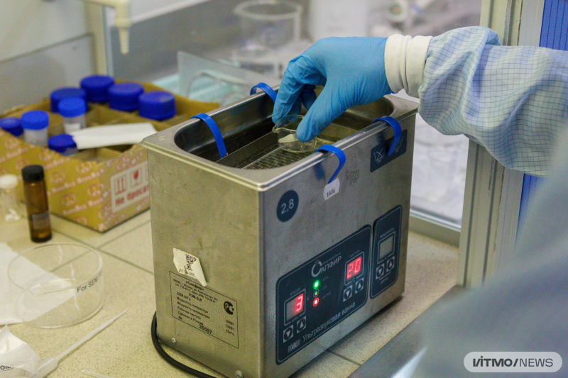
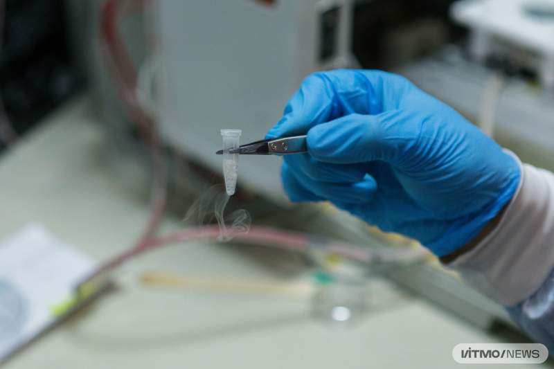
2D MOF crystals are placed into a vial with solvent dimethylformamide; the vial is then placed into an ultrasound bath. Photo by Dmitry Grigoryev / ITMO.NEWS
The layers obtained by sonication. Credit: Small Methods
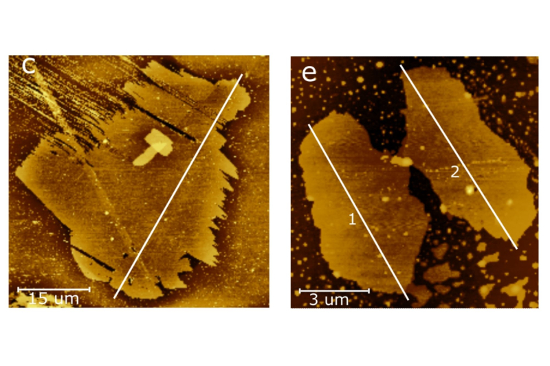
Similar layers were acquired in the second experiment, where the so-called chemical tape was used for exfoliation. In this method, a piece of the tape is used to hold a 2D MOF crystal in place, while the second piece sticks to parts of the crystal, thus removing its layers. Here, the length of a single layer varies from 4 to 25 micrometers and the thickness – from 3 to 60 nanometers; the ratio fluctuated between 330:1 and 1330:1.
Pavel Alekseevskiy applying the tape to a 2D MOF crystal. Photo by Dmitry Grigoryev / ITMO.NEWS
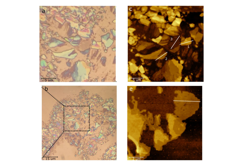
The layers obtained by mechanic (tape) exfoliation. Credit: Small Methods
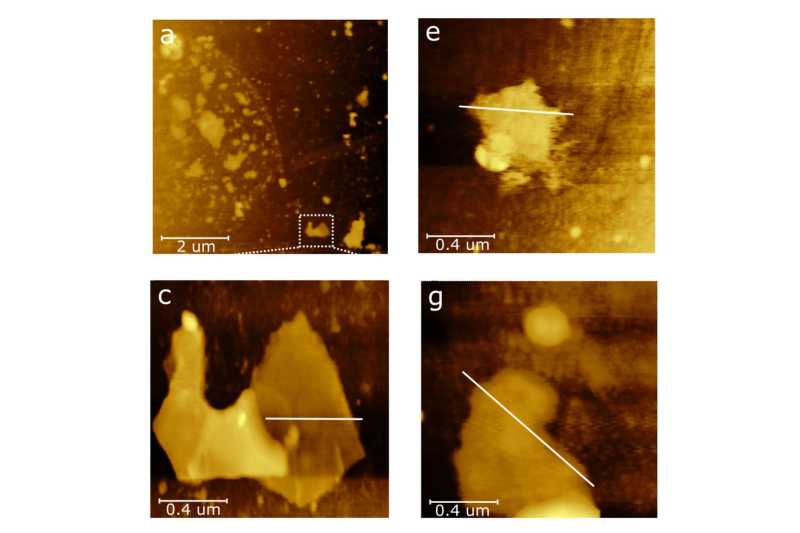
The best results were obtained with the third method, the freeze-thaw – freezing and thawing 2D MOFs in a solvent. Here, the researchers were able to produce layers with record-breaking parameters: 0.5 to 64 micrometers in length and 1-4 nanometers-thick. Such long and thin layers will make for more sensitive chemical and optical devices.
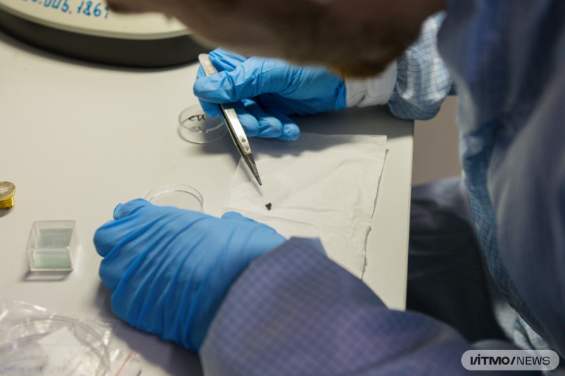
A vial with 2D MOF crystals frozen in liquid nitrogen. Photo by Dmitry Grigoryev / ITMO.NEWS
The layers obtained with the freeze-thaw method. Credit: Small Methods
“We have demonstrated the performance of all three methods, as well as collected statistics on how much time and how many cycles it takes to achieve particular height-to-length ratios, from the smallest ones to the biggest. We used this data to suggest a technological criterion, a parameter that makes it possible to produce a layer that is just a few nanometers in thickness and has a record length-to-height ratio: from 500:1 to 21,300:1. Now, researchers or manufacturers wishing to produce a very long and thin MOF layer for sensors can use a trusted 'recipe' for it,” says Pavel.
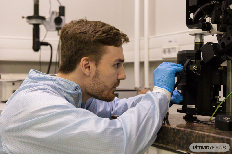
An atomic-force microscope was used to observe the exfoliation results and sizes of layers. Photo by Dmitry Grigoryev / ITMO.NEWS
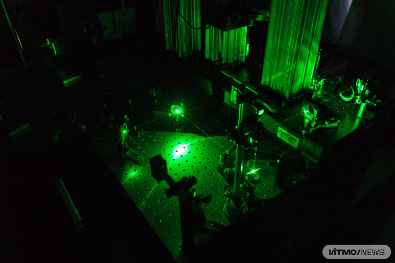
The optical feedback was tested using a laser system. Photo by Dmitry Grigoryev / ITMO.NEWS
What’s next
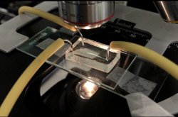
The researchers have also tested how sensitive the acquired layers are to changes in their environment and how their optical feedback can be measured. For this, they tested the layers’ reaction to pairs of 8 solvents in a microfluidic chip. As a result, the 2D MOF layers were able to detect the substances and reacted to them via radiation of different intensity. This means that these layers can be used to develop chemical and optical sensors.
Next, the researchers are planning to develop nano-size closed gas systems and cells. Such devices can be integrated into larger sensors to be installed at labs or production sites working with toxic substances.
“2D MOFs will be placed inside such gas systems. If there are any changes in the environment – for instance, if there are toxic molecules or dangerous solvents, the 2D MOF layer will change its optical feedback; in other words, it will illuminate differently. Moreover, a 2D MOF crystal is autonomous and requires no energy source,” concludes Pavel Alekseevskiy.
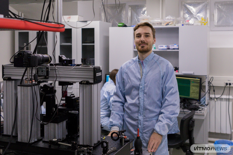
Pavel Alekseevskiy at the lab at ITMO. Photo by Dmitry Grigoryev / ITMO.NEWS
This project is supported by the national program Priority 2030 and grants from the Russian Ministry of Science and Higher Education (No. 075-15-2021-589 and No. 075-15-2021-589).
Reference: Anastasiia Efimova, Pavel Alekseevskiy, Maria Timofeeva, Yuliya Kenzhebayeva, Alina Kuleshova, Irina Koryakina, Dmitry Pavlov, Taisiya Sukhikh, Andrei Potapov, Sergei Shipilovskikh, Nan Li, Valentin Milichko. Exfoliation of 2D Metal-Organic Frameworks: toward Advanced Scalable Materials for Optical Sensing (Small Methods, 2023).