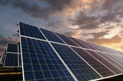
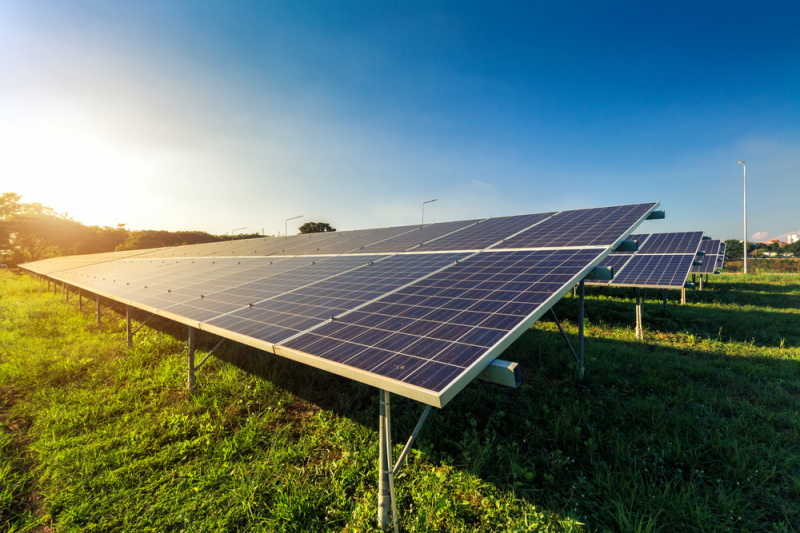
Today, with the rapid exhaustion of hydrocarbon fuel reserves and a growing concern about environmental issues, scientists are paying more and more attention to the development of the so-called “green technologies”. One of the most popular topics in the field is the development of solar energy technologies.
“Hydrocarbons as a traditional source of energy are exhaustible, and their burning leads to the production of carbon dioxide,” says Ivan Mukhin, an ITMO University researcher and the head of a laboratory at Academic University. “Meanwhile, the Sun can be a virtually inexhaustible energy source for our planet. According to the recent calculations, only 1% of the solar energy Earth receives daily would be enough to provide humans with enough electricity for a year! This is why in the future, solar energy has the chance to replace traditional energy sources that depend on burning fossil fuels.”
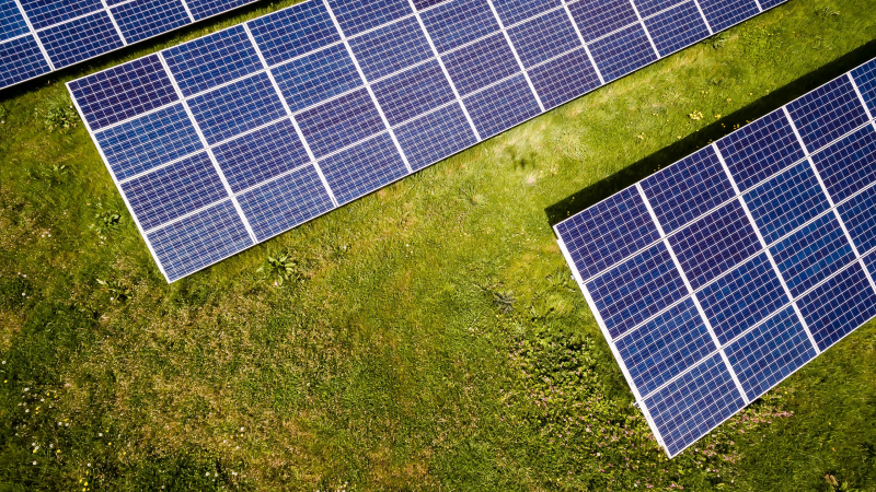
However, wider use of the solar panels is hindered by a number of factors. Conventional silicon solar cells have a relatively low efficiency – less than 20%. More efficient technologies require much more complex semiconductor technologies, which significantly increases the price of the solar cells.
“The most common solar cell technologies are silicon-based,” continues Ivan Mukhin. “This is a relatively cheap and widespread material. The problem is that silicon is an indirect semiconductor and absorbs light rather poorly, which limits its use in efficient solar cells. There are other semiconductor materials, such as A3B5 semiconductor compounds, which consist of elements of the third and fifth groups of the Periodic Table. They are much better at absorbing light but are much more expensive than silicon, which significantly increases the cost of the resulting solar cells. As a result, despite their high efficiency, it’s not profitable to produce them.”
Combining А3В5 and silicon
The St. Petersburg scientists have proposed a solution to this problem. The researchers from ITMO University, St. Petersburg Academic University and the Ioffe Institute showed that A3B5 structures could be grown on inexpensive silicon substrate, providing decrease in the price of multi-junction solar cells.
“Our work focuses on the development of efficient solar cells based on A3B5 materials integrated on silicon-substrate,” comments Ivan Mukhin, an ITMO University researcher, head of a laboratory at Academic University and a co-author of the study. “The main difficulty in the epitaxial synthesis on silicon-substrate is that the deposited semiconductor must have the same crystal lattice parameter as silicon. Roughly speaking, the atoms of this material should be at the same distance from each other as are the silicon atoms. Unfortunately, there are few semiconductors that meet this requirement – one example is gallium phosphide (GaP). However, it’s not very suitable for the fabrication of the solar cells since it has poor sunlight-absorbing property. But if we take GaP and add nitrogen (N), we obtain a solution of GaPN. Even at low N concentrations, this material demonstrates the direct-band property and is great at absorbing light, as well as having the capability to be integrated onto a silicon substrate. At the same time, silicon doesn’t just serve as the building material for the photovoltaic layers – it itself can act as one of the photoactive layers of a solar cell, absorbing light in the infrared range. Zhores Alferov was one of the first to voice the idea of combining ASB5 structures and silicon.”
Working at the laboratory, the scientists were able to obtain the top layer of the solar cell, integrated onto a silicon substrate. With increase of the photoactive layers number the efficiency of the solar cell grows, as each layer absorbs its part of the solar spectrum.
“We haven’t managed to create the final multi-junction cell yet, but together with our colleagues we’ve made a big leap forward in integration of A3B5 on silicon for photovoltaic applications,” adds Ivan Mukhin. “At the same time, rather complex molecular beam epitaxy methods were used to grow the structure. This is a method for the synthesis of thin layers of a highly crystaline semiconductor.”
Prospects
As of now, the researchers have developed the first small prototype of a solar cell based on the А3В5 on silicon-substrate . Now they are working on the development of the solar cell that would consist of several photoactive layers. Such solar cells will be significantly more effective at absorbing sunlight and generating electricity.
“We’ve learned to grow the topmost layer. This material system can potentially also be used for intermediate layers. If you add arsenic, you obtain quaternary GaPNAs alloy, and from it several junctions operating in different parts of the solar spectrum can be grown on a silicon substrate. As demonstrated in our previous work, the potential efficiency of such solar cells can exceed 40% under light concentration, which is 1.5 times higher than that of modern Si technologies,” concludes Ivan Mukhin.
Reference: Liliia N.Dvoretckaia, Alexey D.Bolshakov, Alexey M.Mozharov, Maxim S.Sobolev, Demid A.Kirilenko, Artem I.Baranov, Vladimir Mikhailovskii, Vladimir V.Neplokh, Ivan A.Morozov, Vladimir V.Fedorov, Ivan S.Mukhin, “GaNP-based photovoltaic device integrated on Si substrate”, Solar Energy Materials and Solar Cells, 2020