Perovskites are semiconductor compounds with the general formula ABX₃ that are currently being studied as promising materials for solar cells and flexible displays. They absorb and emit light efficiently, but remain fairly fragile: repeated bending of perovskite-based devices leads to the accumulation of microcracks, which can eventually cause the devices to fail quickly. To determine whether a nanoparticle can withstand repeated bending and compression in a real-world object, scientists need to measure its Young’s modulus, a quantity that indicates how strongly a material resists deformation. The lower the Young’s modulus, the more flexible the material – and therefore the better suited it is, for example, to foldable devices.
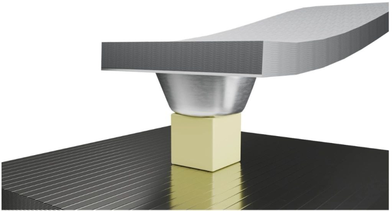
Typically, the mechanical properties of materials are determined with indentors, hard tips of measuring devices that are pressed into a sample. However, even the smallest indentors are too big compared to a single nanoparticle, which makes it impossible to use them to apply pressure to a nanocrystal. A different approach is needed to measure the elasticity of single nanoparticles. ITMO researchers used an atomic force microscope that makes it possible to work with nanometer-scale materials. However, they made its sharp needle that can destroy the fragile nanocrystal blunt, turning it into a flat miniature press.
This made it possible to compress the nanocube more evenly than with a sharp probe. However, later it turned out that because of particle surface irregularities and a slight rounding of the needle, the pressure still wasn’t spreading homogenously. As a result, there was an error in the calculations: it appeared that the smaller the particle, the more durable it is, even though the material’s durability shouldn’t depend on its size.
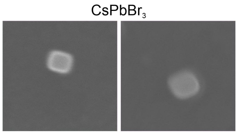
Images of nanoparticles in an electron microscope. Credit: the paper's authors
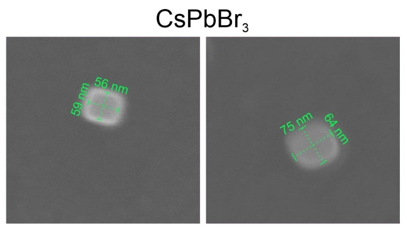
Images of nanoparticles in an electron microscope. Credit: the paper's authors
To eliminate the influence of these factors and obtain accurate Young’s modulus values, the physicists transferred the experiment to a computer environment in the next stage of their work. They created precise 3D models of each particle and the atomic force microscope probe in COMSOL Multiphysics, accounted for the probe’s 20-degree tilt, and ran a compression simulation. They then adjusted the material parameters in the model until the virtual curve showing the particle’s compression as a function of the probe position matched the experimental curve recorded with the actual microscope. This approach made it possible to distinguish geometry-related errors from the material’s true mechanical properties.
The team have already applied this method to measure the durability values for two perovskite compounds: CsPbBr₃ and CsPbCl₃. These are semiconductor materials based on caesium, lead, and halogenes – bromine and chlorine. They can effectively absorb and emit light, which is why they are actively studied for potential application in flexible electronics. As a result, regardless of the crystal’s size, the bromine compound’s Young’s modulus was 16 gigapascal and the chlorine compound’s – 24 gigapascal. This means that perovskites are moderately durable while also being sufficiently malleable, which is important for developing flexible devices. In the future, to assess the material’s behavior under repeated bending comprehensively, the scientists will need to conduct additional tests to determine how well it can withstand a large number of recurring deformations without breaking.
“When we compress a nanoparticle, its mechanical and electronic properties change: electrons require less energy to split from an atom and start moving inside the crystal. This affects the material’s electron structure and its light-emitting capacity. Such changes are important in practice. Understanding the connection between deformation and perovskite properties will allow us to design more sensitive pressure sensors and flexible sensors. Moreover, in the future, optical sensors can be developed based on the changes in a material’s luminescence under compression; such sensors will respond to significant pressure by changing color,” explains Vladislav Kalinichenko, the paper’s first author.
Vladislav Kalinichenko. Credit: Dmitry Grigoryev / ITMO NEWS
The developed method is suitable for measuring the elasticity of any cubic or rectangular nanomaterials, for example, nanoparticles made of metals or semiconductors. In the future, this data could be used to design sensors and memory elements – mechanically sensitive memristors. This will also require measuring the electrical properties of the materials, including piezoelectric properties, which means their ability to generate an electrical charge when compressed or bent.
In the nearest future, the team is planning to expand the method to complex studies with an atomic force microscope, making it possible to measure Young’s modulus alongside other electrical properties of materials. With this approach, it will be possible to acquire electric and mechanical data in a single measurement on a single device, without transporting the sample to different equipment. Thus, it will be possible to evaluate how nanoparticles behave in real devices under pressure. The approach will also be tested to study memristors. Understanding their properties in the future will help create more reliable and energy efficient computational devices, including processors, flexible chips, and data storage devices.
This study was supported by Russian Science Foundation grants No. 24-79-10131 and No. 24-62-00022.
The concept of the study was suggested by Alexandra Furasova, a senior researcher at the Faculty of Physics, and Prokhor Alekseev, an associate professor at the faculty. Compression modelling in COMSOL was accomplished by Vladislav Kalinichenko and Abolfazl Mahmoodpoor, an engineer and a junior researcher at the faculty respectively; they are members of Sergey Makarov’s research group. Quantum-mechanical DFT calculations were conducted by Iuliia Melchakova, a researcher at the faculty, and Alexandr Tsvigun, a student of the Bachelor’s program Applied and Theoretical Physics. Synthesis and sample characterization was done by Kseniya Gasnikova, a student in the Master’s program Photonics and Spintronics.