Tailoring of the near‐field properties of nanostructures is a significant task for the control of radiation of nanoscale light sources as well as for sensing applications. In the recent years, such tasks have been solved by specialists working in the field of plasmonics where different metal particles are used to control light. With the development of dielectric nanophotonics, scientists managed to overcome particular restrictions of plasmonics that had to do with losses on optical frequencies. Not so long ago, scientists have come up with a new relevant concept that has to do with creating hybrid systems which combine the benefits of metals and dielectrics and have enhanced properties that are essential from the practical standpoint (for instance, nonlinear optical properties, unidirectional scattering and the like).

A plasmonic or dielectric nanoparticle can act as a transmitting nanoantenna that converts the localized electromagnetic field into freely propagating waves, or as a receiving antenna that converts the energy of the external electromagnetic field into strongly localized modes. The most noteworthy effects can be attained when the nanoantennas are positioned in clusters, or oligomers (an oligomer is several nanoantennas grouped in a particular manner).
It is possible to control the distribution of oligomers’ near fields by affecting the incident wave: at particular configurations of its polarization (radial or azimuthal), the response of the oligomer in the near field gets reconfigured. Still, in order to attain the desired response, it is necessary to influence the exciting radiation, which is associated with particular technical issues.

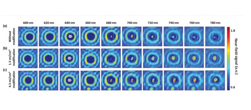
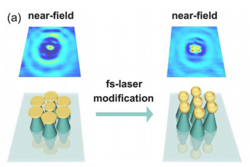
A team of scientists from ITMO's Faculty of Physics and Engineering in collaboration with researchers from Saint Petersburg Academic University have developed a fully optical method for reconfiguring the near field. In their research, they have demonstrated a modification of the near-field pattern in hybrid gold‐silicon oligomers by femtosecond laser reshaping.
“Using a laser greatly simplifies the process: you map the near-field distribution once, and then you work with that. Hybrid structures are created by standard lithography methods, and then you just apply femtosecond laser radiation to modify them. In addition to the above, you don't have to use the more time-consuming and hazardous chemical methods, additional equipment and other complex methods," explains Yali Sun, PhD student at ITMO's Faculty of Physics and Engineering, the article's first author. “The results of our experiments show that even a moderate influence of a femtosecond laser that has close to zero effect on the scattering properties in the far-field region of oligomers results in a considerable reconfiguration of their near field.”

The proposed approach makes hybrid oligomers a promising platform for developing new data recording devices, sensors, and in the coming years, optical chips that will make use of optical signals instead of electric ones, which will allow to increase the channel performance and data density, adds Dmitry Zuev, research fellow at ITMO's Faculty of Physics and Engineering and the corresponding author of the article. According to him, several major companies already showed their interest in ITMO scientists' studies in the field of hybrid nanostructures. In future, the specialists are planning to continue their research in the field of studying and applying metal-dielectric structures in nanophotonic systems.
Reference: (https://onlinelibrary.wiley.com/doi/full/10.1002/lpor.201800274): Reconfigurable Near-field Enhancement with Hybrid Metal-Dielectric Oligomers, Yali Sun, Ivan Sinev, Anastasia Zalogina, Eduard Ageev, Hadi Shamkhi, Filipp Komissarenko, Ivan Morozov, Sergey Lepeshov, Valentin Milichko, Sergey Makarov, Ivan Mukhin and Dmitry Zuev, Laser & Photonics Reviews, 02 January 2019, issue 1800274, doi: 10.1002/lpor.201800274.


