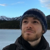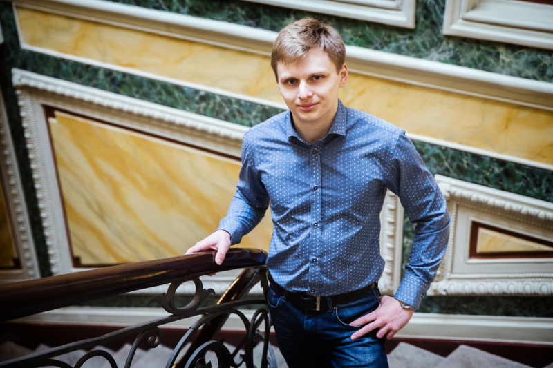
Nikita Teplyakov is a 2020 graduate of the Master’s program Physics and Technology of Nanostructures with an h-index of 11. In 2018, his Bachelor’s thesis was named Russia’s best graduation thesis of the year in the Photonics category.
As a Master’s student, he was the recipient of Presidential and Government scholarships. In his second year, Nikita worked at one of the laboratories of the Swiss Federal Institute of Technology Lausanne (rated the world’s 18th top university by QS) – all thanks to yet another Presidential scholarship. Recently, he was accepted into a PhD program at Imperial College London (rated 8th by QS). Nikita Teplyakov spoke to ITMO.NEWS about his experiences, how he discovered science, and why stereotypes about scientists aren’t always right.
How did you come to choose photonics as your field of study?
When I was making that choice, I was interested in novelty. Photonics is a relatively young field that’s barely covered by the school curriculum. You only barely learn about photons in the final years.
Did you want to be a scientist when you were in school?
I never had that dream, especially since there are lots of stereotypes about scientists in our society. Namely concerning their income level and future prospects. For that reason, I wasn’t going to get a fully fundamental education that would only be useful in academia; I was thinking about what could come in handy in the industry. Today, I can say that those stereotypes can and should be dismantled.
Was that why you chose ITMO University?
That’s right. In 2014, ITMO University gave me the impression of a university where people don’t just do science, but delve into the latest discoveries in photonics. And that they look at these discoveries not only from the point of view of fundamental science, but through a practical lens, too, which helps graduates become viable specialists.
What was the most memorable about your studies?
I have this memory from my first year: we came to class and started to learn about actual science, not the stuff we were told in school. And those were truly niche disciplines in the field of nanostructure physics. I was amazed and drawn to that.
Another thing I remember is doing research at the International Research and Educational Center for Physics of Nanostructures. In my first year, too. I was surprised they’d let us do research at this stage in our studies. It showed a great degree of trust in students, which, in my opinion, pays off in the end.
Speaking of research: did working on nearly 30 research papers leave any room for other activities?
I can’t say I completely abandoned my hobbies and friends, but I won’t lie, either – it’s impossible to contribute to over 20 articles without spending most of your time and energy on research. There are two key factors that made this possible. First, I was and still am interested in the subject of my research; and secondly, the university pays its researchers well. Having a source of income as a Bachelor’s student, of course, motivated me to keep working.
Your Bachelor’s thesis was named the best photonics thesis of 2018. What was it about?
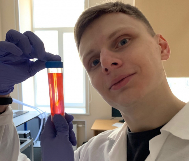
I conducted research on chiral nanocrystals at the International Research and Educational Center for Physics of Nanostructures. Those are nanocrystals that change when mirrored and therefore exist as “left” and “right” particles. They have various applications in physics and medicine, as many drug components can be chiral and have different effects on humans. For instance, the “left” molecules of a substance could be curative, while the “right” ones are poisonous. Chiral nanocrystals let us separate those molecules.
Was this the subject of your research as a Master’s student, too?
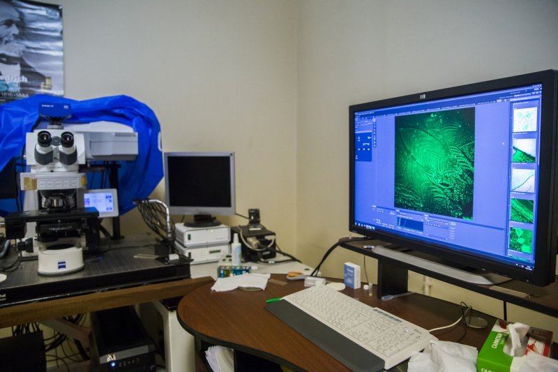
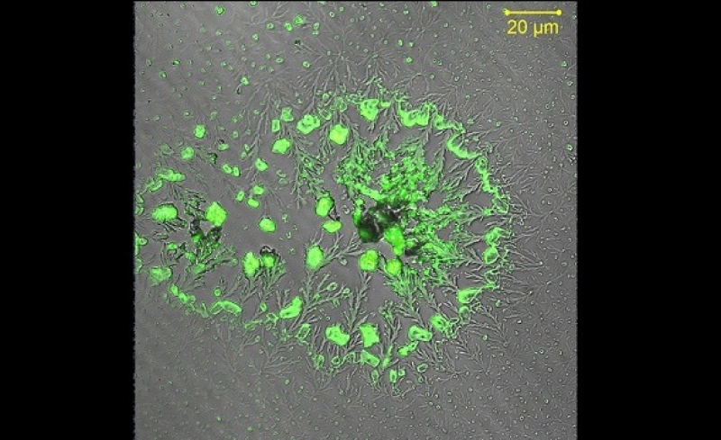
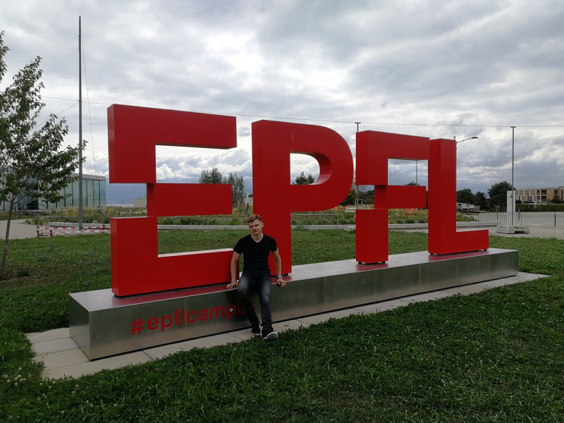
I stayed in the same field, but moved slightly towards carbon nanostructures. Due to their lack of toxic elements, they are some of the most promising materials. Generally, we were interested in modeling the optical properties of such materials. Another question, which half of the thesis is dedicated to, is how we could produce the desired optical response from these nanostructures. I wrote the second part at the Swiss Federal Institute of Technology Lausanne (École polytechnique fédérale de Lausanne, EPFL), where I worked on an adjacent subject, specifically the study of new two-dimensional materials – such as multi-layer graphene.
Were you there on an exchange?
Not really. I was awarded a Presidential scholarship and went there to study, but with an emphasis at working at a laboratory under the guidance of a specific professor. In the fall semester, I attended classes to rack up the required credits (it only took three disciplines), and I spend the rest of my time working at the laboratory.
So you had to have an application approved personally by a professor?
That’s right. I picked an expert in an adjacent field: it let me expand my qualifications while also not straying too far from my previous research. That was the point of the scholarship: my task was to do the same sort of full-fledged research as what I would’ve done at ITMO.
What fundamental differences have you noticed between the working processes of Russian and Swiss laboratories or research teams?
I’d say that in Switzerland the work mode is more “relaxed.” What I mean is that scientists there can work on one subject for several years without publishing anything if they believe that the results so far aren’t worth reporting. In other words, they’re not subject to such strict requirements in terms of published articles.
In my view, it’s a double-edged sword. Perhaps Russian researchers produce more material, some great, some in need of improvement. In Switzerland, you don’t have to worry about having enough material and instead focus on the quality. Another aspect is the well-known Swiss precision and meticulousness. People there are very strict about the quality of the end result: a project that’s ready to be published could be sent back for reworking more than once.
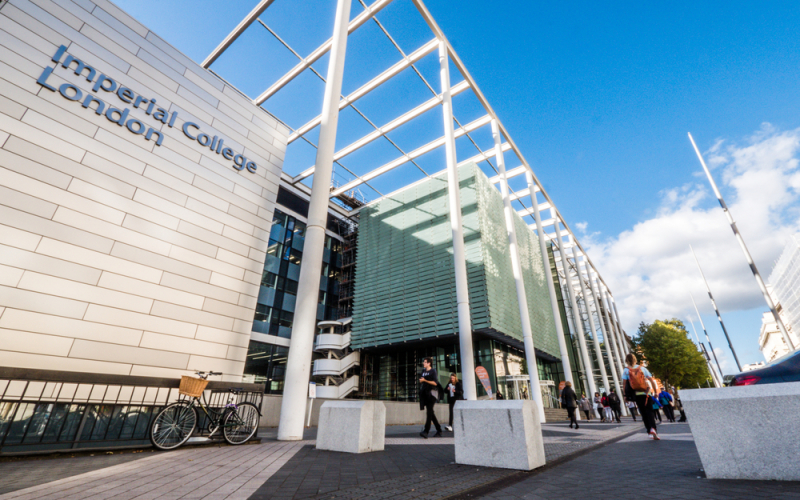
You got accepted into a PhD program at Imperial College London. Was that difficult?
I’d say that, considering the results of my studies as a Bachelor’s and Master’s student at ITMO University, it was rather easy. The selection process wasn’t very challenging: I got in touch with some professors who worked at universities I liked, sent them my CV, passed a short interview, applied for a scholarship, and awaited the results.
Why that university in particular?
First of all, it is one of the UK’s and the world’s top universities; I applied to several of its counterparts, including Cambridge. But the professor I’ll be working with there is one of the most well-known specialists in their field, and that had a major influence on my decision.
You're about to start three intense years of studies and research, but looking even further ahead – what would you love to do in the future?
I’m not sure yet whether I’ll continue my research or go into the industry. The thing is, I’m in theoretical physics and it’s not easy to find practical applications for it outside of science. Even though theoretical physicists are welcomed in fields like data science and finance because of the way they think and analyze things, I wouldn’t want to leave physics behind. In any case, I’m sure that the knowledge and experience I’ve gained at ITMO University will benefit my future career more than once.