This is already the fifth time that the summer school is being held as part of a collaborative framework of the Röntgen-Angström-Cluster (RAC) and the Ioffe-Röntgen-Institute (IRI), a joint initiative between Russia, Sweden and Germany. The three countries are trying to pave the way in using the best X-rays and neutron sources in material science.

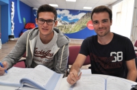
Participants of the 5th International Summer School RACIRI-2017. Source: raciri.org
The school is designed for students in their final years of university, postgraduates, and young scientists from the three partner countries. This year 87 people participated in the school. Each year, the organizers choose new relevant topics related to research in the field of material and life sciences. The theme is always related to maximizing the potential of existing and emerging installations (synchrotron radiation sources, x-ray lasers, neutron sources).
“This is the first time I’m participating in this school. When I applied, I mentioned my work at the UniFEL center, where we are preparing to work with XFEL (european x-ray free-electron laser). The theme of the school this year was about applying X-ray sources and neutron radiation-based X-ray synchrotrons and lasers, so I think that’s why I was accepted”, explained Nikita Prasolov.
As part of the school, participants attended lectures designed to improve their understanding of the fundamentals in advanced materials design. Special lectures were held on the use of neutron and x-ray methods, and meetings with internationally renowned scientists and world-leading experts in relevant scientific fields, as well as poster sessions and student contests.
The school was as rich as you can get: each day the participants listened to five lectures. During one of the lectures, they learned about the latest news regarding the XFEL construction – the most powerful X-ray set-up of its time. Numerous countries were involved in its construction, including Russia (who contributed about 27%). As soon as the laser is ready, scientists expect that there will be a boom of research conducted on it.
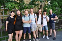
 Participants of the 5th International Summer School RACIRI-2017. Source: social media
During the first three days, the school organizers prepared a competition - a poster session. The students could, with the help of posters, get to know each other’s projects, and then vote for the project they liked the best. Another student competition, Science Slam, was also held, in which 5 teams gave creative oral presentations about their research projects. One team sang a song and played guitar, another showed how they work with small-angle neutron scattering (where one teammate was the source, and the other was a specimen for analysis), and so on.
“I work with molecular dynamics, and plan to simulate the interaction of x-ray radiation with a surface such as graphene”, shared the PhD student, Prasolov.
His main subject is modelling molecular dynamic methods of nanoindentation. Now he is studying the interaction between atoms with the help of computer simulation.
“I modeled the interaction process of the atomic force microscope probe with a gallium arsenide (GaAs) surface, mainly the indentation. It was interesting for us to see the origins of this effect, as triboelectrification (surface electrification under mechanical action). This effect occurs when scanning the surface with a probe, in the process it creates an electrification, or static. The static is observed without making a significant destruction to the surface, that is, the force applied to the probe, and the depth of the indentation must be small”, explained the PhD student.
This is not the first year Nikita Prasolov is studying about the effect of changing surface potential (effect of triboelectrification). The fact is that the nature of this effect is not yet clear. On a global scale, there are very few who study the triboelectrification effect.
 Nikita Prasolov
It was discovered that, by changing the surface potential, it is possible to change the crystal growth process on the substrate. This can be used in microelectronics. Modern methods of epitaxial growth of semiconductors - molecular beam (growing in conditions of ultra-high vacuum semiconductors structures with atomic-smooth surfaces) and the MOS-hydride epitaxy (deposition of organometallic compounds from the gas phase), are sensitive to the physical and chemical surface properties, especially electrification. A particularly strong effect can be seen during the growth of membranes of nanometer thickness, or the growth of of self-assembled quantum dots, that is, with a controlled concentration and geometric dimensions.
“There is an assumption that the surface electric potential changes as a result of the generation of deep level point defects in the band gap, that can recharge (can accept a charge and transfer it). For example, there are vacancies (in crystallography, a vacancy is where in an ideal crystal there should be an atom but there isn’t), in subsurface layers, or the atom occupies an intermediate position between lattice sites, which modifies the potential surface. I’d like to see, with the help of molecular dynamics, the moment when the point defects appear.” explains the young scientist.
Soon after the school ended, the participants were taken on a tour of the synchrotron installation MAX IV and the construction of the new European Spallation Source (ESS) in Lund, Sweden.


